Heating element, heating base plate, method for making heating base plate, microswitch and fluid sensor

A technology for heating elements and manufacturing methods, applied in electrical switches, thermal relays, electrical components, etc., can solve the problems of reduced reliability of protective films, redundant steps, deterioration of thermal efficiency, etc., and achieves good durability, improved heating efficiency, and size high precision effect

Inactive Publication Date: 2005-01-19
SEIKO EPSON CORP
View PDF3 Cites 0 Cited by
  • Summary
  • Abstract
  • Description
  • Claims
  • Application Information

AI Technical Summary

Problems solved by technology

Usually, in such a case, in order to prevent the formation of amalgam, the surface of the heating element, for example, is covered with Si 3 N 4 , SiO 2 etc. to form a protective film, but the steps for forming this protective film are redundant
In addition, sometimes the reliability is reduced due to the coverage problem of the protective film
In addition, thermal efficiency may deteriorate due to the thermal capacity of the protective film itself

Method used


Image

  • Heating element, heating base plate, method for making heating base plate, microswitch and fluid sensor
  • Heating element, heating base plate, method for making heating base plate, microswitch and fluid sensor
  • Heating element, heating base plate, method for making heating base plate, microswitch and fluid sensor

Examples


no. 1 Embodiment approach

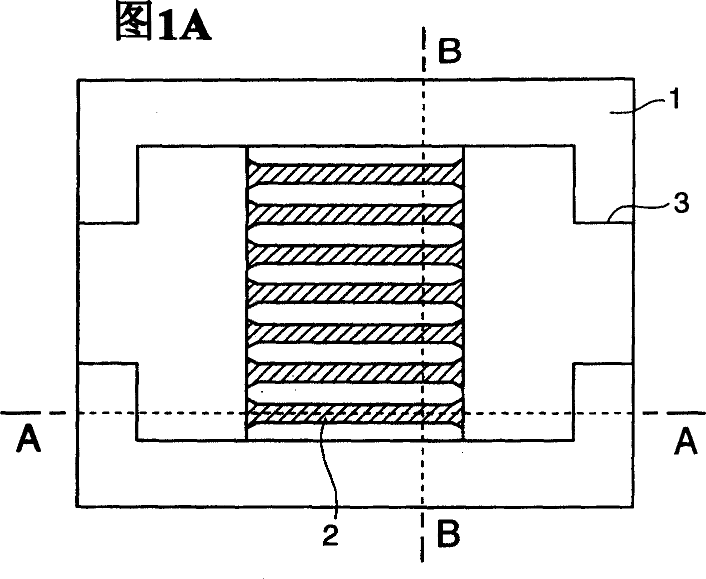
[0053] FIG. 1 is a schematic diagram of a substrate having a heating element according to a first embodiment of the present invention, showing an enlarged portion of the substrate where the heating element is installed. FIG. 1A is a view of a substrate seen from above. also, Figure 1B It is a sectional view taken along the line A-A in FIG. 1A . Figure 1C It is a sectional view along the line B-B in FIG. 1A.

[0054] The substrate 1 is a substrate made of silicon (hereinafter referred to as a silicon substrate). The heating part (membrane) 2 is actually a heating element that can carry heat. In this embodiment, as a material of the heating portion 2 , silicon in which impurities have been diffused is used. As the impurity, for example, boron (B: boron) is preferable. Silicon diffused with impurities such as boron has conductivity.

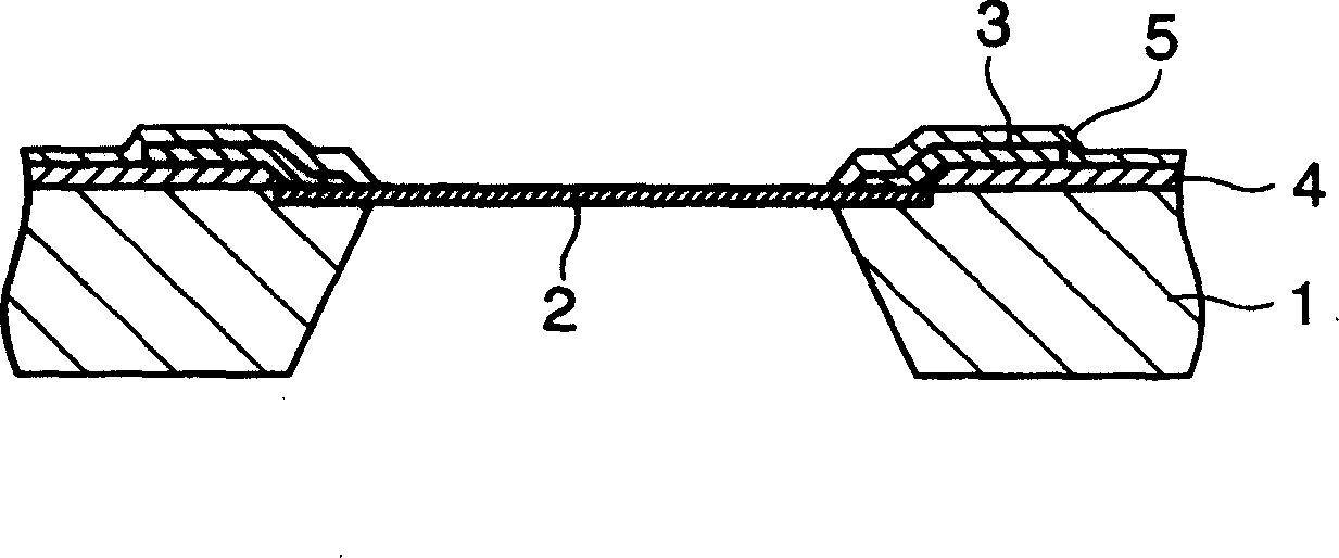
[0055] Among them, such as Figure 1B As shown, the heating part 2 is a bridge structure suspended (suspended) by the silicon substrate 1 . ...

no. 2 Embodiment approach

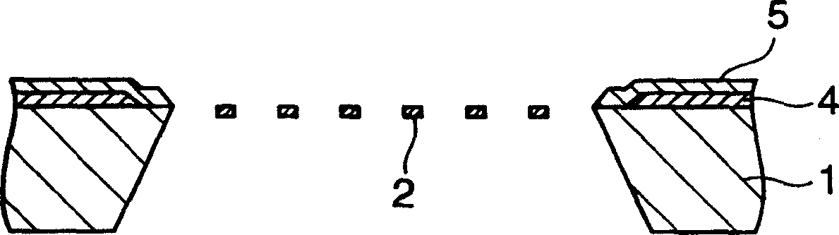
[0070] Figure 5A to Figure 5F and Figure 6G to Figure 6M It is a schematic diagram which shows the manufacturing process of the heating element of this embodiment. In the figure, each figure shown on the right shows a sectional view corresponding to the direction of the A-A line shown in FIG. 1A, and each figure shown on the left shows a sectional view corresponding to the direction of the B-B line shown in FIG. 1A. In this embodiment, the oxide film (SiO 2 ) 11 after pattern making, form a boron doped layer 14 on the surface (hereinafter referred to as heating surface 12) constituting the heating portion 2, after forming the protective film 5 for wet etching protection on the heating surface 12, from the heating surface 12 Dry etching and wet etching of silicon are performed on the substrate 1 to obtain a heating element having a cavity shape of the heating portion 2 .

[0071] Hereinafter, a method of manufacturing a heating element will be described with reference to F...

no. 3 Embodiment approach

[0105] Figure 10A with Figure 10B It is a figure which shows the film-forming process of the protective film 5 which concerns on the 3rd Embodiment of this invention. In the above-mentioned first embodiment, in Figure 3I In the shown steps, the film as the protective film 5 is processed in the illustrated shape by performing half etching. In this embodiment, by forming a film as the protective film 5 in two stages, it is processed into Figure 3I the shape shown.

[0106] Therefore, the processing is performed in the following steps instead of the one described in the first embodiment Figure 3I A step of. First, film formation treatment is performed on the insulating film 4 and the wiring 3 by a plasma CVD device, such as Figure 10A As shown, the first-stage film 5a is formed into a film. Then, the film formation process is performed again by the plasma CVD device, such as Figure 10B As shown, by forming the film 5b of the second stage, it is processed into Fig...


PUM


Abstract

The invention provides a good-stability and -durability heating component and a substrate as well as its high-efficiency and -accuracy making method and the device using them. It uses at least one part electroconductive silicon substrate diffused with impurities like B and so on as the material for etching processing, integrally makes a heating part, where the heating part is provided with one or many narrow slits without angle parts or with circular ones. At the same time, for controlling the heating state of the heating part and it forms a concave part arranged in the bottom part.

Description

technical field [0001] The present invention relates to, for example, a heat generating element suitable for a micro switch (relay), a sensor, etc., especially a small device, and a manufacturing method thereof. Background technique [0002] Conventionally, an electrical component (device) called a switch that performs electrical switching has been used. With the development of electronic technology, such switches have been miniaturized in order to be incorporated into electronic components such as measuring devices, and are provided as so-called micro switches (also called micro relays), for example. [0003] Microswitches mechanically open and close solid electrodes through conductive liquid metal, for example, and perform electrode switching operations of opening and closing electric contacts and electrically connecting them. In a microswitch, for example, a plurality of electrodes are exposed and molded at predetermined positions on the inner wall of an elongated channe...

Claims


Application Information

Patent Timeline
Patent Type & Authority Applications(China)
IPC IPC(8): H01H29/00H01H61/00H01H61/01
Inventor 荒川克治藤井正宽小枝周史
Owner SEIKO EPSON CORP
Why Eureka
Try Eureka