An orthogonal light path type fluorescent detection device for microchip analysis
A fluorescence detection and orthogonal detection technology, which is applied in measuring devices, analyzing materials, and analyzing materials through optical means, can solve problems such as expensive, difficult to miniaturize, and complex optical system structure, and achieve low cost and reduced Effects of light scattering and high detection sensitivity
- Summary
- Abstract
- Description
- Claims
- Application Information
AI Technical Summary
Problems solved by technology
Method used
Image
Examples
Embodiment 1
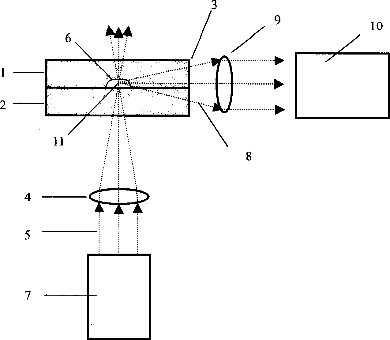
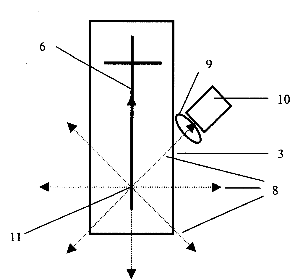
[0024] Refer to attached figure 1 , The microchip is composed of upper 1 and lower 2 glass sheets, and the thickness of the glass sheets is 1.7 mm. A channel is processed on the upper sheet 1 by photomask and wet etching technology, and the width of the microchannel 6 is 60 microns, and the depth is 20 microns. The classic high-temperature bonding method is used to realize the permanent sealing of the upper 1 and lower 2 pieces. A microfluidic chip with a length of 60 mm and a width of 15 mm was obtained. In the present embodiment, the excitation light source 7 is a semiconductor pump laser of 473nm; the excitation light 5 emitted by the laser is focused by the condenser objective lens 4, and enters the chip microchannel 6 from a direction perpendicular to the plane of the lower chip 2 of the chip; 11 emitted, the fluorescence 8 emitted from the chip side wall 3 is collected by the collection objective lens 9 positioned behind the detection window, and the setting direction ...
Embodiment 2
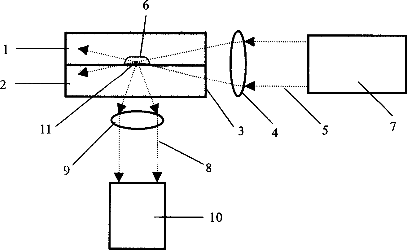
[0027] Refer to attached image 3 After the excitation light 5 emitted by the light source 7 is converged by the focusing objective lens 4, it is incident from the side wall 3 of the chip in a direction perpendicular to the microchannel 6 of the chip; the fluorescent light 8 emitted from the direction perpendicular to the lower chip 2 of the chip is selected, and collected The objective lens 9 collects the stray light, and the stray light is filtered out by the optical filter, and finally the fluorescent signal is detected by the photodetector 10 .
[0028] Figure 4 It is the channel configuration diagram of the micro-analysis chip according to the preferred embodiment 1 of the present invention. The separation channel part of the microchannel 6 on the chip is designed with a bend, near the edge of the side wall 3 of the chip at the end detection area 12, in order to shorten the distance of fluorescence from the light spot to the detection window and improve the collection e...
PUM
| Property | Measurement | Unit |
|---|---|---|
| Thickness | aaaaa | aaaaa |
| Thickness | aaaaa | aaaaa |
| Length | aaaaa | aaaaa |
Abstract
Description
Claims
Application Information


