Active element array architecture

A technology of active components and array structures, applied in optics, instruments, transistors, etc., can solve problems such as unfavorable liquid crystal displays

Inactive Publication Date: 2005-01-26
AU OPTRONICS CORP
View PDF0 Cites 1 Cited by
  • Summary
  • Abstract
  • Description
  • Claims
  • Application Information

AI Technical Summary

Problems solved by technology

However, this is very unfavorable for the instant-on and ready-

Method used


Image

  • Active element array architecture
  • Active element array architecture
  • Active element array architecture

Examples


Embodiment Construction

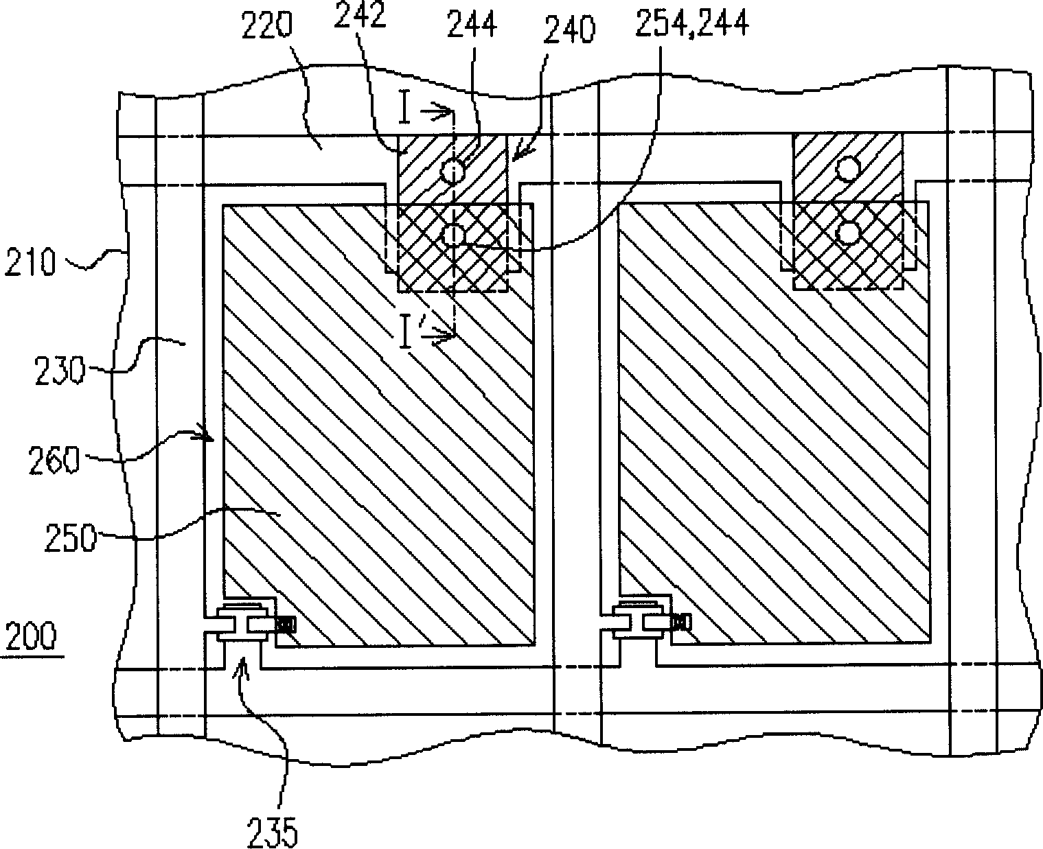
[0038] figure 2 What is shown is a schematic diagram of the active element array structure in the preferred embodiment proposed according to the present invention. Please refer to figure 2 As shown, the active element array structure 200 is composed of a substrate 210 and a plurality of scanning wirings 220, a plurality of data wirings 230, a plurality of active elements 235, a plurality of storage capacitors 240 and a plurality of pixel electrodes 250 disposed on the substrate 210. constituted. Wherein, the scan lines 220 are arranged parallel to each other on the substrate 210 , and the data lines 230 are arranged parallel to each other on the substrate 210 , and the scan lines 210 are perpendicular to the data lines 220 . The area between any two adjacent scan lines 220 and any two adjacent data lines 230 is a pixel area 260 . The active element 235 , such as a thin film transistor, is disposed at the intersection of the scan wiring 220 and the data wiring 230 , and th...


PUM


Abstract

A initiating elements array structure comprises a base plate, multiple scanning lines on the plate; multiple data layouts; multiple initiating elements; multiple reservoir capacitors and multiple picture element electrodes, wherein, each reservoir capacitor has a upper electrode with at least one hole on it and the direction of field through the hole is at an angle with the friction assigning direction of optics self-compensation birefraction LCD coat. When exerting electricity field to optics self-compensation birefraction LCD molecules, the LCD molecules form twisted array and then quickly turn from spreading status to bending status and then though elastic force transmission between LCD molecules to speed up conversion time of all LCD molecules to fulfill the purpose of rapid warm-up of the LCD display.

Description

technical field [0001] The present invention relates to an active element array structure, and in particular to an active element array suitable for quickly transforming an optical self-compensating birefringent liquid crystal layer from a stretched state into a twisted arrangement and then into a curved state. structure. Background technique [0002] The rapid progress of the multimedia society is mostly due to the rapid progress of semiconductor components or man-machine display devices. As far as the display is concerned, the cathode ray tube (Cathode Ray Tube, CRT) has been monopolizing the display market in recent years because of its excellent display quality and economical efficiency. However, for the environment where individuals operate most terminals / display devices on the table, or from the perspective of environmental protection, if the trend of energy saving is predicted, cathode ray tubes still have many problems in terms of space utilization and energy consum...

Claims


Application Information

Patent Timeline
IPC IPC(8): G02F1/13363G02F1/1343G02F1/136H01L29/786
Inventor 张庭瑞
Owner AU OPTRONICS CORP
Why Eureka
Try Eureka