
Substrate processing apparatus and method for adjusting a substrate transfer position

A technology of substrate processing device and handover position, which is applied in the direction of photolithography process exposure device, transportation and packaging, lighting and heating equipment, etc., can solve the problems of time-consuming, uneconomical, discrete sensitivity, etc. Effect

Active Publication Date: 2005-02-02
TOKYO ELECTRON LTD
View PDF1 Cites 23 Cited by
  • Summary
  • Abstract
  • Description
  • Claims
  • Application Information

AI Technical Summary

Problems solved by technology

[0008] However, in the above-mentioned teaching, it is not economical to provide sensors 21 for all the units of the substrate processing apparatus, so the actual situation is that the operator uses the common sensor 21 to adjust the target processing unit when performing the teaching.
In particular, in the above-mentioned coating / developing device in which a plurality of processing units are assembled, each processing unit is miniaturized in order to reduce the occupied area of ​​the device, so the operator adjusts the sensor 21 in the unit while performing axis alignment. time consuming problem
[0009] In addition, in the case of using the light reflective sensor 21, the sensitivity of the sensor 21 may vary due to the surrounding atmosphere such as dust or illuminance, so there is a concern that the edge of the wafer W cannot be detected with high accuracy.

Method used


Image

  • Substrate processing apparatus and method for adjusting a substrate transfer position
  • Substrate processing apparatus and method for adjusting a substrate transfer position
  • Substrate processing apparatus and method for adjusting a substrate transfer position

Examples


Embodiment Construction

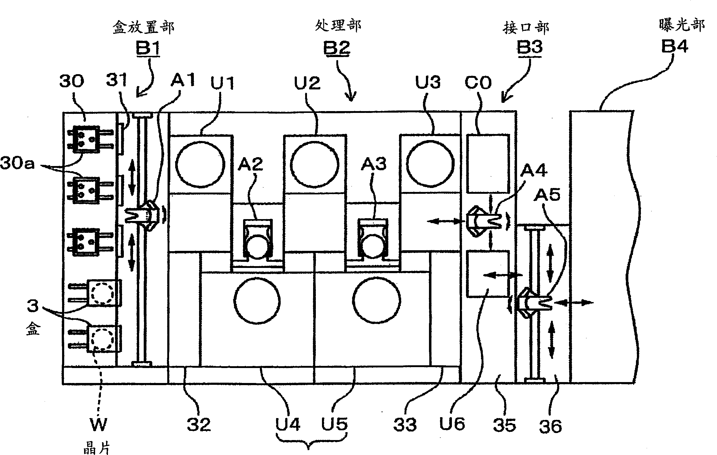
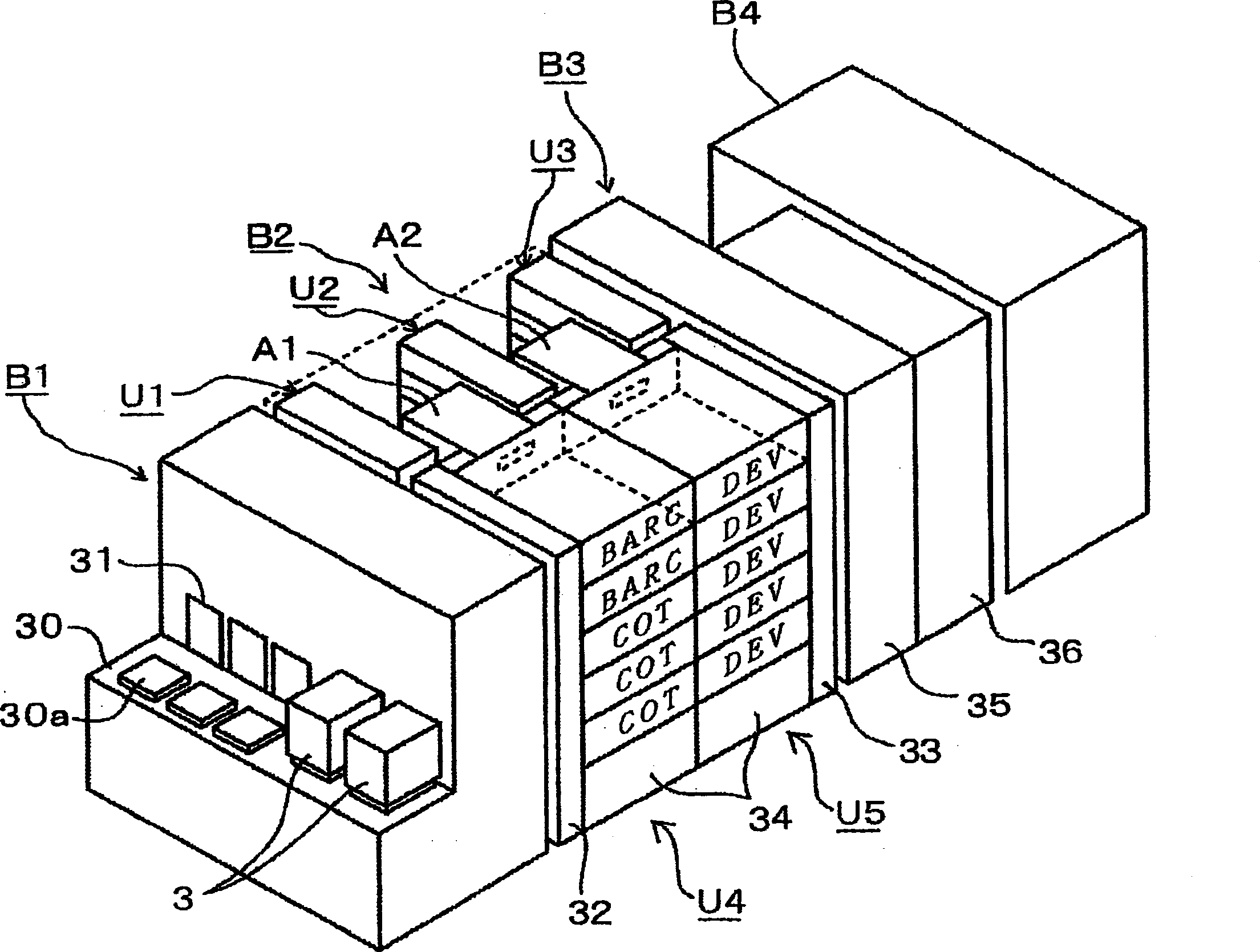
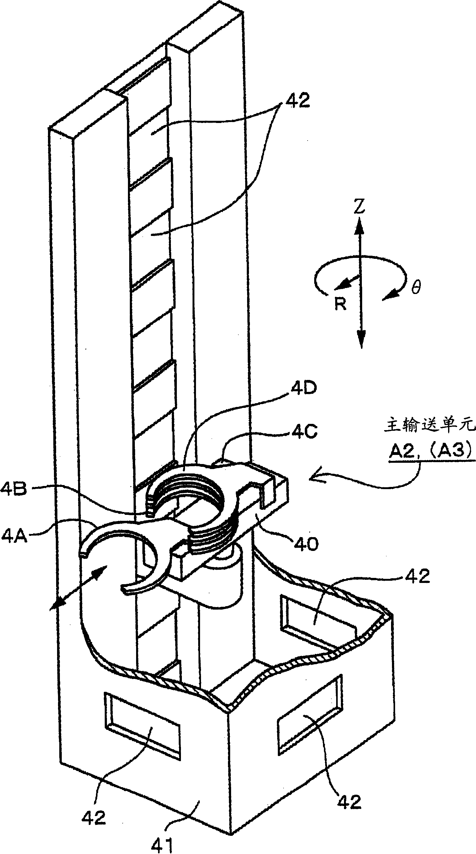
[0074] First refer to figure 1 and figure 2 A coating and developing apparatus according to an embodiment of the substrate processing apparatus of the present invention will be described. B1 in the figure is a cassette loading section for loading and unloading cassettes 3 that house 13 wafers W as substrates in a hermetically sealed manner. As seen from the table 30, there is an opening and closing unit 31 provided on the front wall surface; In addition, the rear side of the cassette loading part B1 is connected to the processing part B2, and the processing part B2 is provided with: rack units U1, U2, U3 in which the units of the heating and cooling system are multi-staged; Liquid processing units U4, U5 that perform predetermined liquid processing; and main transfer units A2, A3 that transfer wafers W to and from each unit. That is, the main transfer units A2 and A3 are configured to be able to access adjacent units, and the wafer W can freely move from the rack unit U1 ...


PUM


Abstract

To align a substrate with high accuracy for a short time in acquiring the data of a substrate delivery position to a substrate holding part beforehand with respect to a substrate conveying means conveying the substrate in and out of a processing unit performing predetermined processes to the substrate. With respect to a mark that is formed on the surface of a substrate for alignment delivered to a substrate holding part by a substrate conveying means, the positions of the marks are respectively imaged before and after the time when the substrate holding part is rotated 180[deg.], for example. After the misregistration between the positions of the center of the substrate and the rotational center of the substrate holding part is calculated on the basis of the positional data of this mark, the existence of the misregistration calculated by this means is decided. There is such a constitution that the substrate is rearranged to the substrate conveying means in such a manner that the center of the substrate coincides with the rotational center of the substrate holding part at the time when it is decided that there is misregistration.

Description

technical field [0001] The present invention relates to a substrate processing apparatus that acquires position data of a substrate transfer unit in advance when delivering a substrate to a processing unit for performing predetermined processing such as resist application, development, and heating on a substrate held on a substrate holding unit. , and a method for adjusting the transfer position of the substrate. Background technique [0002] Conventionally, in the photoresist process as one of the semiconductor manufacturing processes, for example, a resist is applied in a thin film on the surface of a semiconductor wafer (hereinafter referred to as wafer), and the resist is exposed in a predetermined pattern. After that, development is performed to form a predetermined mask pattern. Generally, such a treatment is performed by using a substrate processing apparatus in which an exposure apparatus is connected to an application / development apparatus for applying and developi...

Claims


Application Information

Patent Timeline
IPC IPC(8): H01L21/68B65G49/07G03F7/20H01L21/027H01L21/677
Inventor 伊藤和彦石丸和俊大仓淳木下道生道木裕一
Owner TOKYO ELECTRON LTD
Features
  • Generate Ideas
  • Intellectual Property
  • Life Sciences
  • Materials
  • Tech Scout
  • Unparalleled Data Quality
  • Higher Quality Content
  • 60% Fewer Hallucinations
Learn More