Semiconductor integrated circuit device

A technology of integrated circuits and semiconductors, which is used in the manufacture of semiconductor devices, circuits, and semiconductor/solid-state devices.

Active Publication Date: 2005-02-02
PANNOVA SEMIC
View PDF1 Cites 4 Cited by
  • Summary
  • Abstract
  • Description
  • Claims
  • Application Information

AI Technical Summary

Problems solved by technology

[0005] However, the above-mentioned conventional semiconductor integrated circuit devices can only reduce the stress disturbance in a specific element pattern within the active region between differentially operated transistors like p-channel transistors and n-channel transistors.

Method used


Image

  • Semiconductor integrated circuit device
  • Semiconductor integrated circuit device
  • Semiconductor integrated circuit device

Examples


no. 1 approach

[0042] Hereinafter, a first embodiment of the present invention will be described with reference to the drawings.

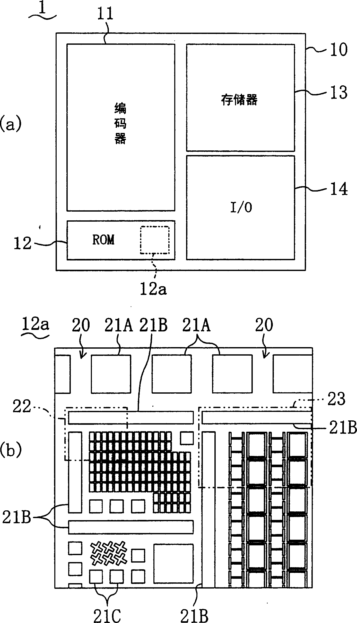
[0043] figure 1 (a) shows a schematic plan configuration of the semiconductor integrated circuit device according to the first embodiment of the present invention.

[0044] Such as figure 1 As shown in (a), the semiconductor integrated circuit device 1 of the first embodiment includes, for example, an encoder unit 11 formed on a semiconductor substrate 10 made of silicon and having an MPEG (Motion Picture Experts Group: Motion Picture Experts Group) encoding function; ROM unit 12 having ROM (Read Only Memory: read only memory) function; memory unit 13; I / O unit 14, which realizes the output / input (I / O) function with the outside.

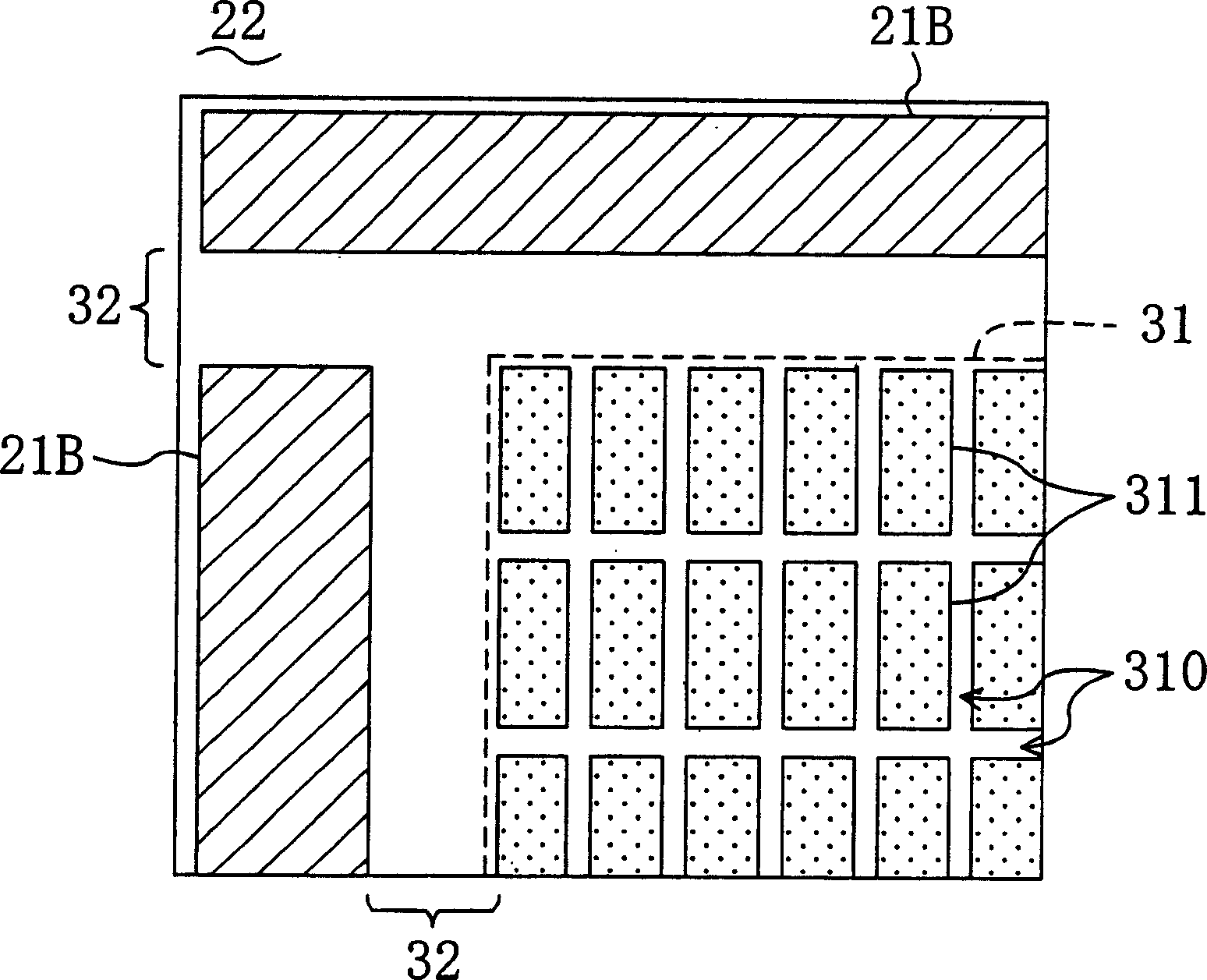
[0045] figure 1 (b) means figure 1 (a) An enlarged view of an arbitrary region 12a in the ROM portion 12 shown. Such as figure 1 As shown in (b), in the region 12a, a plurality of dummy active regions 21A, 21B, and 21C partit...

no. 2 approach

[0074] A second embodiment of the present invention will be described below with reference to the drawings.

[0075] Figure 8 (a) A plan view showing a corner of the SRAM circuit of the semiconductor integrated circuit device according to the second embodiment of the present invention, Figure 8 (b) means Figure 8 (a) The stress value of the active region and the change in the threshold voltage of the transistor formed in the stressed active region. exist Figure 8 (a), with Figure 7 The constituent elements shown in (a) that are the same as the constituent elements are given the same reference numerals.

[0076] Figure 8 (a) means figure 1 (b) The second area 23 shown in (b), that is, the enlarged view of the corner of the SRAM circuit.

[0077] Such as Figure 8 As shown in (a), the semiconductor integrated circuit device according to the second embodiment includes a dummy active region 21B and an SRAM circuit forming portion 41 arranged inside the dummy active ...

no. 3 approach

[0089] A third embodiment of the present invention will be described below with reference to the drawings.

[0090] Figure 10 (a) A plan view showing a corner of the SRAM circuit of the semiconductor integrated circuit device according to the third embodiment of the present invention. Figure 10 (b) means Figure 10 (a) The stress value of the active region and the change in the threshold voltage of the transistor formed in the stressed active region. exist Figure 10 (a), with Figure 9 The constituent elements shown in (a) that are the same as the constituent elements are given the same reference numerals.

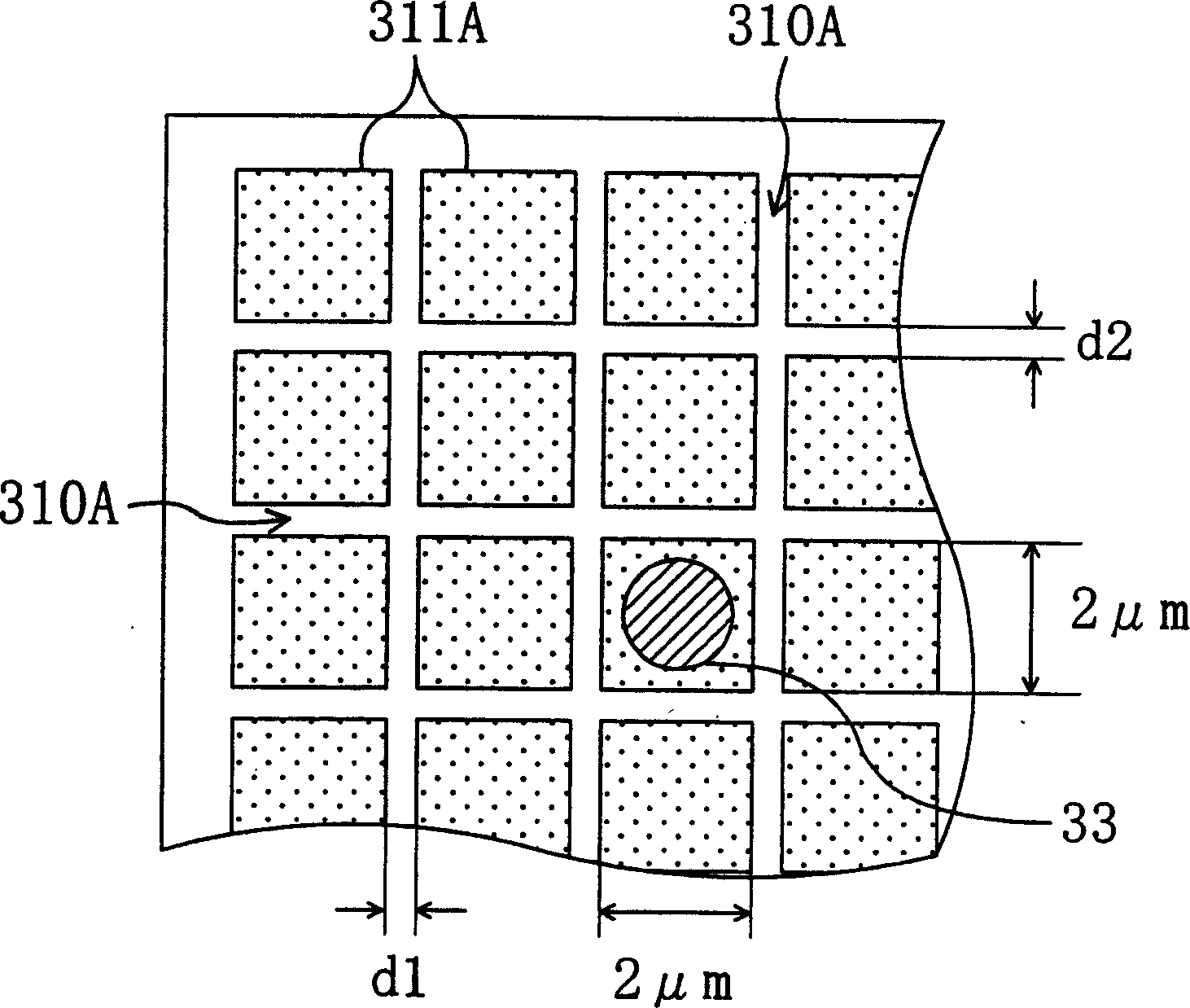
[0091] Such as Figure 10 As shown in (a), in the third embodiment, the dummy active region 21B is also divided into a plurality, and like a modified example of the second embodiment, the width d1 of the outer STI region 42 in the x direction and the width d1 in the y direction The width d3 and the interval d5 in the x direction and the interval d6 in the y direct...


PUM


Abstract

To reduce and moreover prevent change in the operation characteristic of semiconductor elements due to difference in stress generated at the end and the center by reducing difference of stress at the end and center of the active region of a device. A semiconductor element formed in the active region (311) included in a first element forming area (31a) (stress varying region 101) in a peripheral circuit forming area (31) is not electrically driven but only a semiconductor element in a second element forming area (31b) (stress stable region 102) is driven electrically. Therefore, the second element forming area (31b) in the peripheral circuit forming area (31) is isolated from the STI region (32) at the external side of element, and thereby is not easily influenced by a compressed stress.

Description

technical field [0001] The present invention relates to a semiconductor integrated circuit device (LSI), and more particularly to a semiconductor integrated circuit device which prevents or suppresses changes in device operating characteristics caused by stress applied to an active region of the device by an element isolation region. Background technique [0002] refer to Figure 12 A conventional semiconductor integrated circuit device will be described (for example, refer to Patent Document 1). [0003] Such as Figure 12 (a) and Figure 12 As shown in (b), in a dynamic random access memory (DRAM) device formed on a semiconductor substrate 200 made of silicon, between a memory cell 210 and a peripheral circuit 213, a p-channel transistor region 211 of a sense amplifier is formed. and the n-channel transistor region 212 are spaced apart from each other, and element isolation (STI) regions extending parallel to each other are formed between the memory cell 210, the p-channel...

Claims


Application Information

Patent Timeline
Patent Type & Authority Applications(China)
IPC IPC(8): H01L21/76H01L21/822H01L21/8242H01L27/00H01L27/02H01L27/04H01L27/08H01L27/10H01L27/108H01L29/76
CPCH01L27/0207
Inventor 山田雅留奥野泰利
Owner PANNOVA SEMIC
Why Eureka
Try Eureka