Ultrasonic printed circuit board transducer

A technology for circuit boards and transducers, applied in the directions of printed circuits, printed circuits, printed circuit manufacturing, etc., can solve the problems of low acoustic performance, transducer expenses, etc., and achieve simple and flexible design, low cost, and easy implementation. Effect

Inactive Publication Date: 2005-02-02
大卫·W·申德尔
View PDF1 Cites 19 Cited by
  • Summary
  • Abstract
  • Description
  • Claims
  • Application Information

AI Technical Summary

Problems solved by technology

[0006] The second issue is that not all markets and applications of capacitive ultrasonic transducers really require the highest bandwidth produced by the micromachining of the transducer
Micromachining of transducers can lead to unnecessary expense when simpler manufacturing methods can provide relatively low but still adequate acoustic performance
[0007] A third problem is trying to fabricate a roughened backplate with a three-dimensional top surface (e.g., spherical) to control the shape of the ultrasonic field generated, and trying to fabricate such a device as a focused transducer without caused by
[0008] The final issue is that whether micromachining or other methods are used to fabricate the backplane, careful attention must be paid to: (a) effective electromagnetic shielding and packaging issues of the backplane; and (b) ease of integration with associated discrete electronic components (usually Hole and Surface Mount Technology (SMT))

Method used


Image

  • Ultrasonic printed circuit board transducer
  • Ultrasonic printed circuit board transducer
  • Ultrasonic printed circuit board transducer

Examples


Embodiment Construction

[0026] In the following description, the same features are given the same reference numerals in the figures.

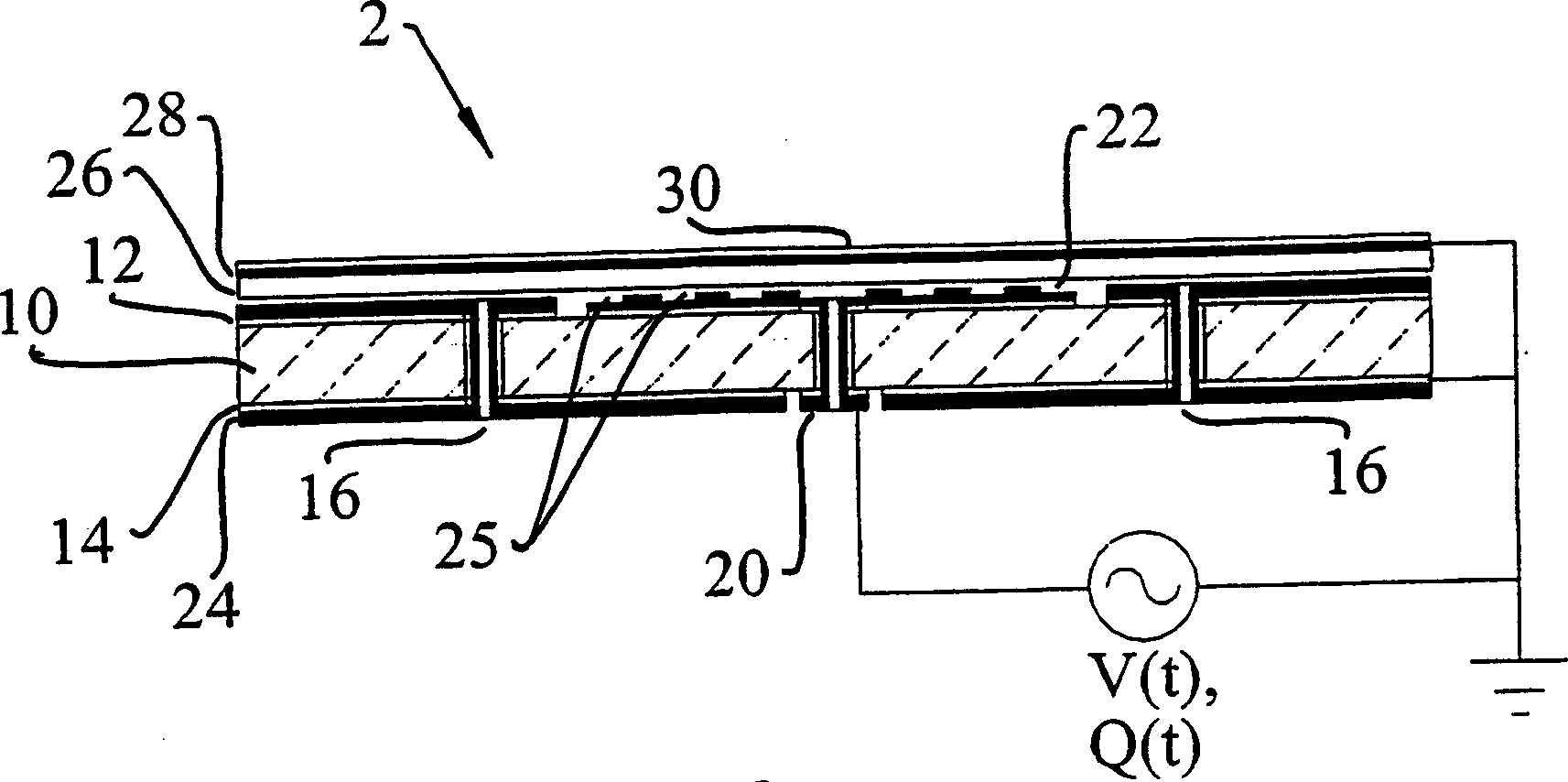
[0027] figure 1 An ultrasonic transducer assembly 2 manufactured according to one aspect of the invention is shown in cross-section. The patterned conductive layers (typically made of copper) on the top side 12 and bottom side 14 of the electrically insulating PCB 10 (typically made of fiber composite material) are fabricated using standard PCB manufacturing processes. The PCB can be rigid or flexible and can be manufactured according to known techniques. The manufacture of flexible PCB can refer to Microflex Circuits similar to 3M TM techniques used in or other flex circuit design techniques. In the present invention these techniques are suitable for the manufacture of transducer assemblies.

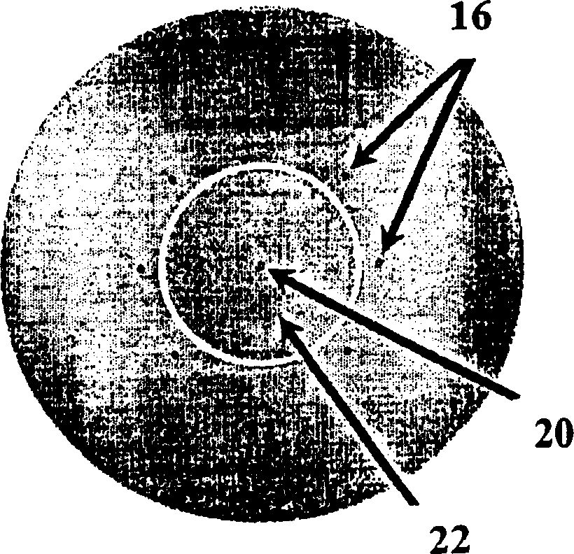
[0028] The through-hole vias 16, 20 for connecting the top surface patterned conductors to the bottom surface patterned conductors are fabricated by first drilling a plural...


PUM


Abstract

There is provided methods for producing an ultrasonic transducer assembly. The methods generally comprise the steps of creating a multi-layered rigid or flexible printed circuit board, having a top surface and bottom surface; creating a patterned conducting layer upon each of the top and bottom surface; creating at least one patterned backplate electrode on the board or as part of a discreet component which is then attached to the board; creating at least one conductive through-hole via integral with the board; roughening at least a portion of each of the at least one backplate to introduce gas pockets in that portion of a surface of the backplate; and attaching thin insulating or dielectric single or multi-layer film on a portion of the board in which the film has an integral conducting surface and in which the conducting surface is configured so as to form a capacitive structure with the at least one backplate.

Description

technical field [0001] The present invention relates to ultrasonic printed circuit board transducer assemblies and exemplary methods of manufacturing the same. Background technique [0002] Methods of fabricating gas-coupled and liquid-coupled ultrasonic capacitive transducers that can operate in a large frequency bandwidth (~40KHz-2MHz) are described in earlier patents (US Patent 5287331 and Canadian Patent 2105647). The method involves fabricating a precisely defined pit structure on the surface of a solid or polymer material as a backplane using micromachining or IC fabrication techniques. These surface pits trap small air pockets when the metallized polymer film is disposed thereon. The polymer film serves as the active element of the device, ie generates and receives ultrasonic waves by vibration. When ultrasonic waves are generated, a time-varying voltage V(t) is applied to the polymer film, and the outer metallized surface of the polymer film is grounded while apply...

Claims


Application Information

Patent Timeline
Patent Type & Authority Applications(China)
IPC IPC(8): H04R19/00B06B1/02H04R31/00H05K1/16H05K3/38H05K3/46
CPCH05K1/162H05K3/4602H05K1/16H05K2201/10083H05K3/382B06B1/0292Y10T29/4908Y10T29/49007Y10T29/49005Y10T29/4913Y10T29/49004Y10T29/49002
Inventor 大卫·W·申德尔
Owner 大卫·W·申德尔
Why Eureka
Try Eureka