High-density chip scale package and method of manufacturing the same

A chip-size packaging and high-density technology, applied in semiconductor/solid-state device manufacturing, electrical components, electrical solid-state devices, etc., can solve problems such as limiting the scope of application

Inactive Publication Date: 2005-02-09
SAMSUNG ELECTRO MECHANICS CO LTD
View PDF1 Cites 9 Cited by
  • Summary
  • Abstract
  • Description
  • Claims
  • Application Information

AI Technical Summary

Problems solved by technology

However, the structure disclosed in the above-mentioned publication has a cooling fan, which limits its applicability

Method used


Image

  • High-density chip scale package and method of manufacturing the same
  • High-density chip scale package and method of manufacturing the same
  • High-density chip scale package and method of manufacturing the same

Examples


Embodiment Construction

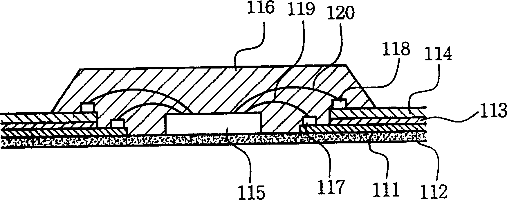
[0051] Figures 3a to 3i A cross-sectional view showing a process of manufacturing a high-density chip-scale package using a heat radiation structure according to a preferred embodiment of the present invention, wherein a die is mounted on the package by wire bonding techniques.

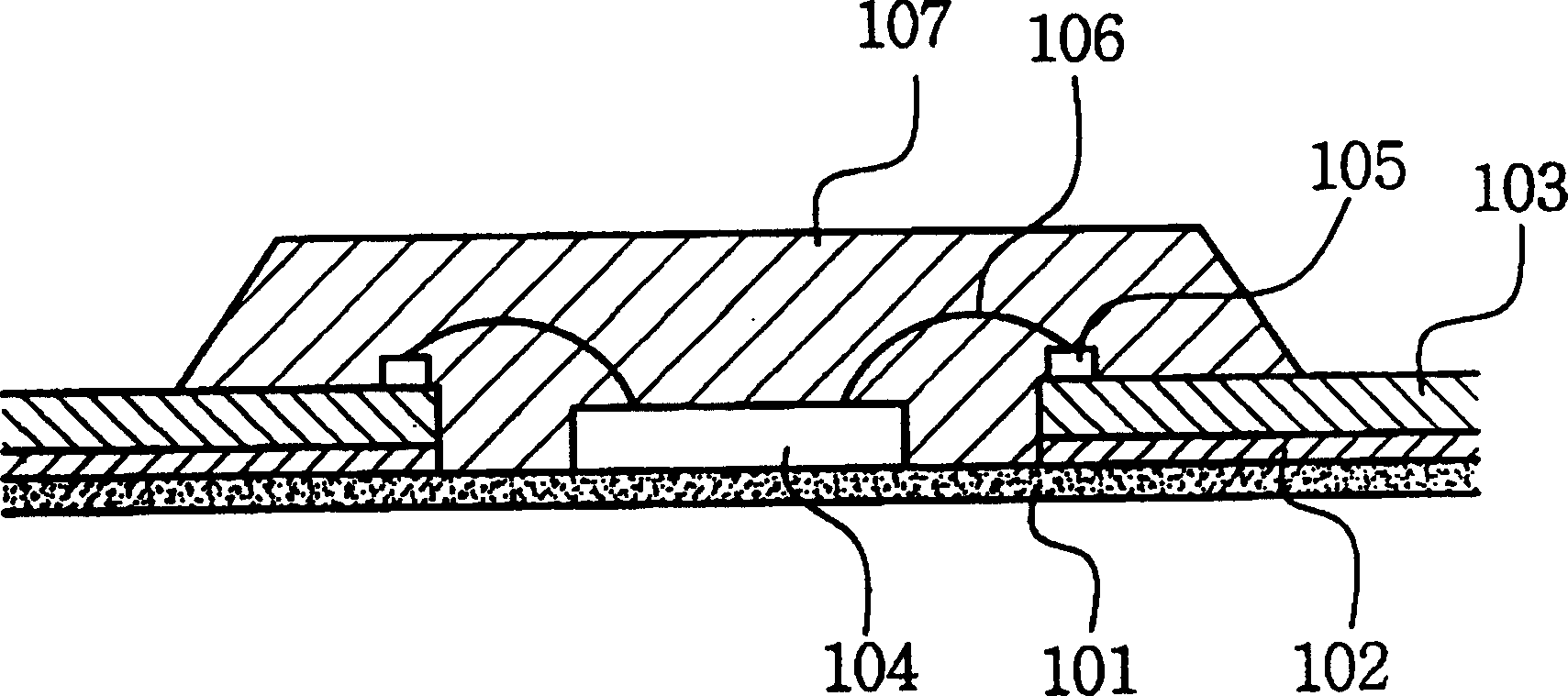
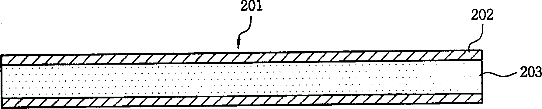
[0052] Figure 3a is a cross-sectional view of a copper-clad thin laminate 301, which is a substrate used in the high-density chip-scale package of the present invention. Such as Figure 3a As shown, the insulating layer 303 is covered with copper foil 302 . There are various copper clad thin laminates. However, a glass / epoxy resin copper-clad thin laminate composed of a reinforcing material obtained by infiltrating an epoxy resin (a mixture of a resin and a hardener) into glass fibers and copper foil is mainly used. In particular, copper-clad thin laminates designated FR-4 are most commonly used. An FR-4 copper-clad thin laminate is used as the copper-clad thin laminate in the present invention,...


PUM


Abstract

Disclosed herein is a high-density chip scale package which is capable of increasing circuit density and expanding a circuit-formable zone. The high-density chip scale package comprises a die having a circuit pattern formed thereon, and a printed circuit board adapted for mounting the die thereon. The printed circuit board has an area 100% to 150% as large as an area of the die, and the printed circuit board has a circuit pattern formed thereon. On the die is mounted a heat sink for radiating heat from the die. Between the printed circuit board and the heat sink is filled an encapsulant for securely connecting the printed circuit board and the heat sink and shielding the printed circuit board from the outside.

Description

technical field [0001] The present invention relates to high-density chip-scale packages capable of increasing circuit density and expanding the area where circuits can be formed, and more particularly to high-density packages that do not require the preparation of cavities and the use of liquid encapsulants in conventional techniques when heat sinks are attached to packages. Chip size packaging, in order to increase circuit density, expand the formable circuit area, enhance the heat radiation efficiency of the heat sink, and can be applied to any kind of chip mounted by wire bonding and flip chip technology. Background technique [0002] As known to those skilled in the art, as the electronics industry is highly developed, electronic devices become smaller while they have increased capacity. Advances in IC chips inevitably lead to an increase in the number of I / O (input / output) of semiconductors. When the number of I / Os of semiconductors increases, a large amount of heat i...

Claims


Application Information

Patent Timeline
Patent Type & Authority Applications(China)
IPC IPC(8): H01L23/12H01L21/56H01L23/34H01L23/433H01L23/498
CPCH01L23/4334H01L2924/0105H01L2924/01082H01L21/56H01L2224/16H01L2224/73215H01L2224/49109H01L2224/73253H01L2924/15311H01L2924/01029H01L2924/01087H01L2224/48091H01L2224/32225H01L24/33H01L2924/01047H01L23/49816H01L24/48H01L2224/73204H01L2924/01079H01L2224/48227H01L2924/01005H01L2924/01033H01L2924/01006H01L24/49H01L2924/01078H01L2224/16225H01L2224/73265H01L2924/3025H01L24/73H01L2224/05599H01L2224/45099H01L2224/85399H01L2224/8592H01L2924/00014H01L2924/12042H01L2924/181H01L2924/00H01L2924/00012H01L2224/45015H01L2924/207H01L23/34
Inventor 郑永熙
Owner SAMSUNG ELECTRO MECHANICS CO LTD
Why Eureka
Try Eureka