

Method of measuring crystal defects in thin SI/SIGE bilayers
A technology for crystal defects and defects, applied in the field of semiconductor device manufacturing, can solve problems such as lack of chemical corrosion technology
- Summary
- Abstract
- Description
- Claims
- Application Information
AI Technical Summary
Problems solved by technology
Method used
Image

Examples
Embodiment Construction
[0021] The invention will be described in more detail with reference to the drawings of the present application, which present a method for characterizing crystal defects in Si / SiGe bilayers. In the drawings, the same and corresponding elements are denoted by the same reference numerals.
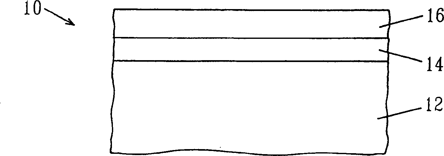
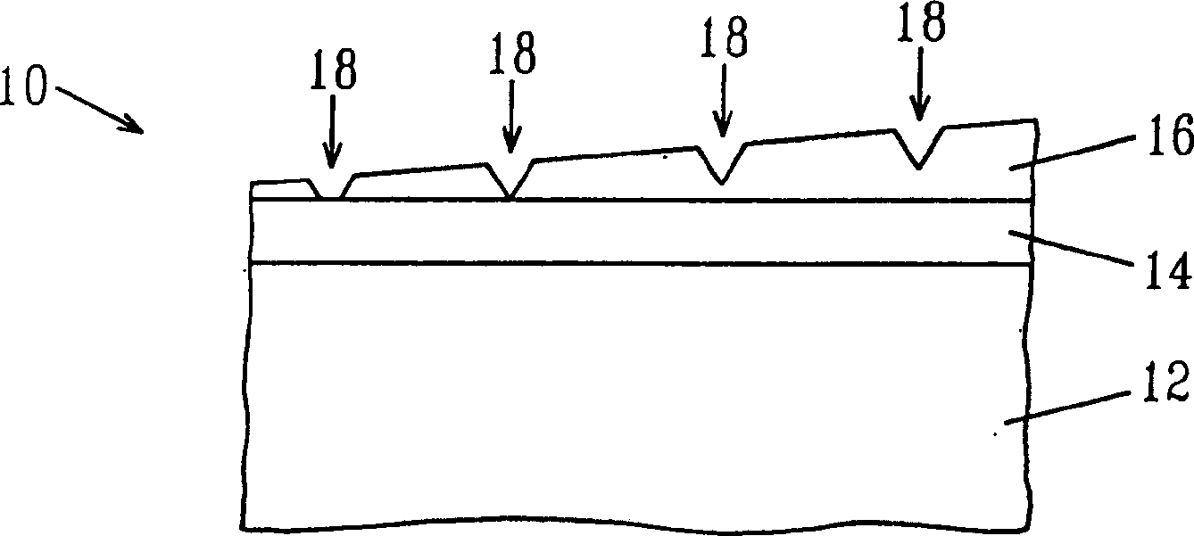
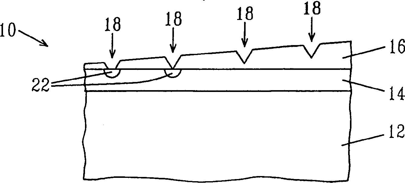
[0022] See first the present invention figure 1 The initial structure shown. Initial structure 10 includes at least Si layer 16 on top of SiGe layer 14 . Initial structure 10 also includes substrate 12 underlying SiGe layer 14 . Substrate 12 may include a bulk Si substrate or any other semiconductor substrate as well as a buried insulating region and a bottom semiconductor layer of a silicon-on-insulator (SOI) substrate; the top SOI layer of the SOI substrate has been used in the formation of the SiGe layer.
[0023] figure 1 The initial structure 10 shown is formed using methods well known to those skilled in the art. For example, the initial structure 10 may be formed by first growing...
PUM
| Property | Measurement | Unit |
|---|---|---|
| Thickness | aaaaa | aaaaa |
Abstract
Description
Claims
Application Information