Transistor based on double barrier tunnel junction resonant tunneling effect
A technology of resonant tunneling and tunnel junction, which is applied in the field of spin transistor devices and can solve problems such as no spin transistor devices yet.
- Summary
- Abstract
- Description
- Claims
- Application Information
AI Technical Summary
Problems solved by technology
Method used
Image
Examples
no. 1 example
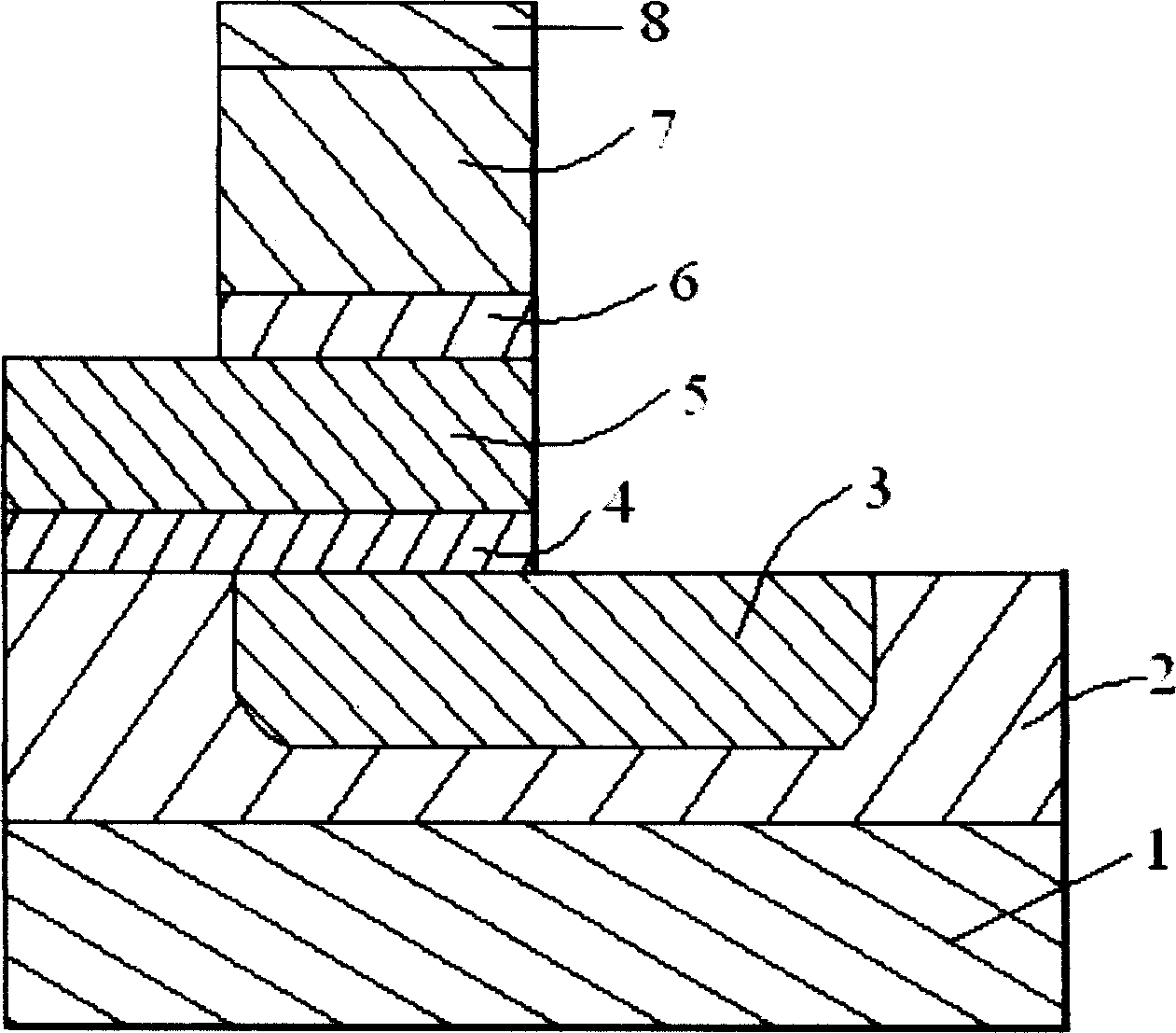
[0017] Such as image 3 Shown by silicon dioxide (SiO 2 ) or similar material is formed on a silicon substrate 1; an emitter 3 made of a magnetic material layer is formed on the insulating layer 2, and the magnetization direction of the emitter 3 is fixed; the first The tunnel barrier layer (barrier layer) 4 is formed on the emitter 3; and an intermediate metal layer or semiconductor layer is formed on the first tunnel barrier layer 4, that is, the base 5; The second tunnel barrier layer (barrier layer) 6; a collector electrode 7 made of ferromagnetic material is formed on the second tunnel barrier layer 6, and the magnetization direction of the collector electrode 7 is free and can be changed with the external magnetic field changes; a protective layer 8 is arranged on the collector electrode 7 .
[0018] It should be noted that the aforementioned emitter 3 is formed on one layer of antiferromagnetism, so that the magnetization position of this layer of magnetic material ca...
no. 2 example
[0023] In this embodiment, the schematic sectional view of the transistor structure is similar to that of the first embodiment. Such as image 3 Shown by silicon dioxide (SiO 2 ) or similar material is formed on a silicon substrate 1; an emitter 3 made of a semi-metallic magnetic material layer is formed on the insulating layer 2, and the magnetization direction of the emitter 3 is fixed; a The first tunnel barrier layer (barrier layer) 4 is formed on the emitter 3; The thickness depends on the chosen material and should be comparable to the mean free path length of the material; a second tunnel barrier (barrier layer) 6 formed above the base 5; a collector made of a semi-metallic magnetic material 7 is formed on the second tunnel barrier layer 6 , the magnetization direction of this layer is free and can change with the external magnetic field; a protective layer 8 is arranged on the collector electrode 77 .
[0024] In the above-mentioned embodiment, the material of the b...
no. 3 example
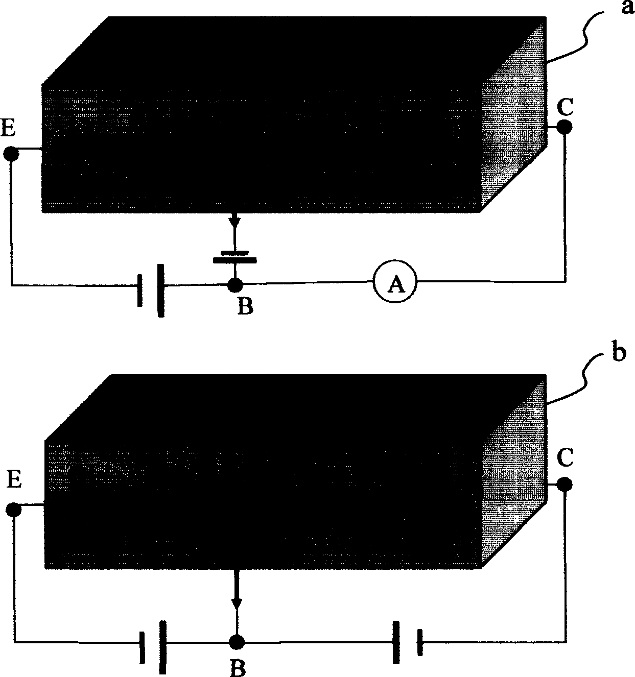
[0027] In the first embodiment and the second embodiment, non-magnetic metal materials or semiconductor materials are used for the base material, and if the material of the base is replaced by a general magnetic material or a semi-metallic magnetic material, due to the properties of the base material The spin-dependent transport characteristics are more conducive to modulating the magnetization direction of the collector through it. In view of this, the third embodiment proposes a spin transistor device in which the base material is a magnetic material. figure 2 The b in it is a schematic diagram of its structure.
[0028] The structure of the transistor of this embodiment is similar to that of the first embodiment. Such as image 3Shown by silicon dioxide (SiO 2 ) or similar material is formed on a silicon substrate 1; an emitter 3 made of a magnetic material layer whose magnetization direction is fixed is formed on the insulating layer 2; a first A tunnel barrier layer ...
PUM
 Abstract
Description
Claims
Application Information


