Helical resonator type plasma processing apparatus

A spiral resonator and plasma technology, applied in the direction of plasma, semiconductor/solid-state device manufacturing, discharge tube, etc., to achieve the effect of improving density uniformity

Inactive Publication Date: 2005-05-11
SAMSUNG ELECTRONICS CO LTD
View PDF0 Cites 22 Cited by
  • Summary
  • Abstract
  • Description
  • Claims
  • Application Information

AI Technical Summary

Problems solved by technology

However, conventional helical resonator plasma processing equipment has shortcomings in adequately controlling the plasma potential for a particular process and processing conditions

Method used


Image

  • Helical resonator type plasma processing apparatus
  • Helical resonator type plasma processing apparatus
  • Helical resonator type plasma processing apparatus

Examples


Embodiment Construction

[0040] The present invention will now be described more fully hereinafter with reference to the accompanying drawings, in which preferred embodiments of the invention are shown by way of example. The same reference numerals identify the same elements throughout the drawings.

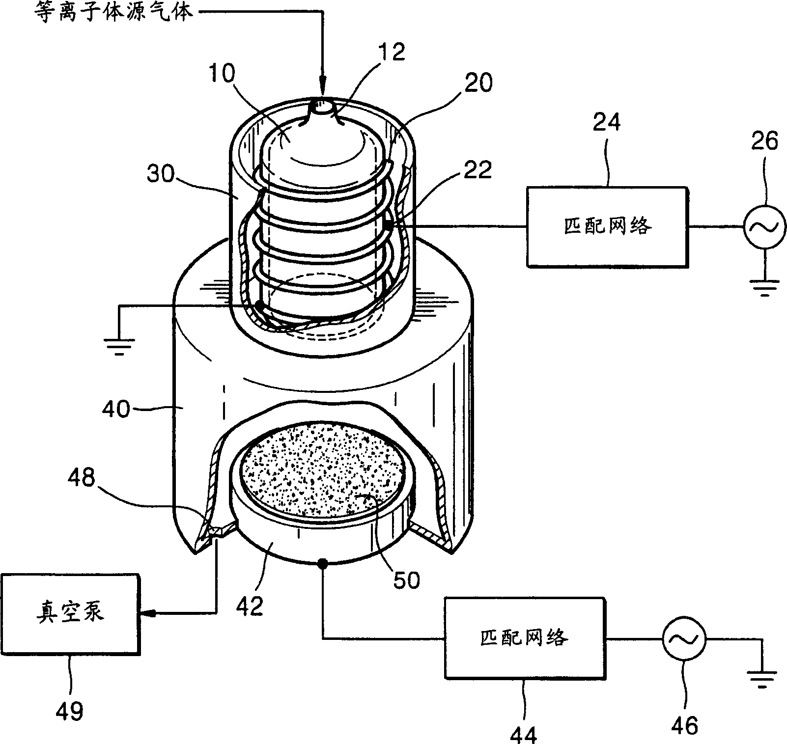
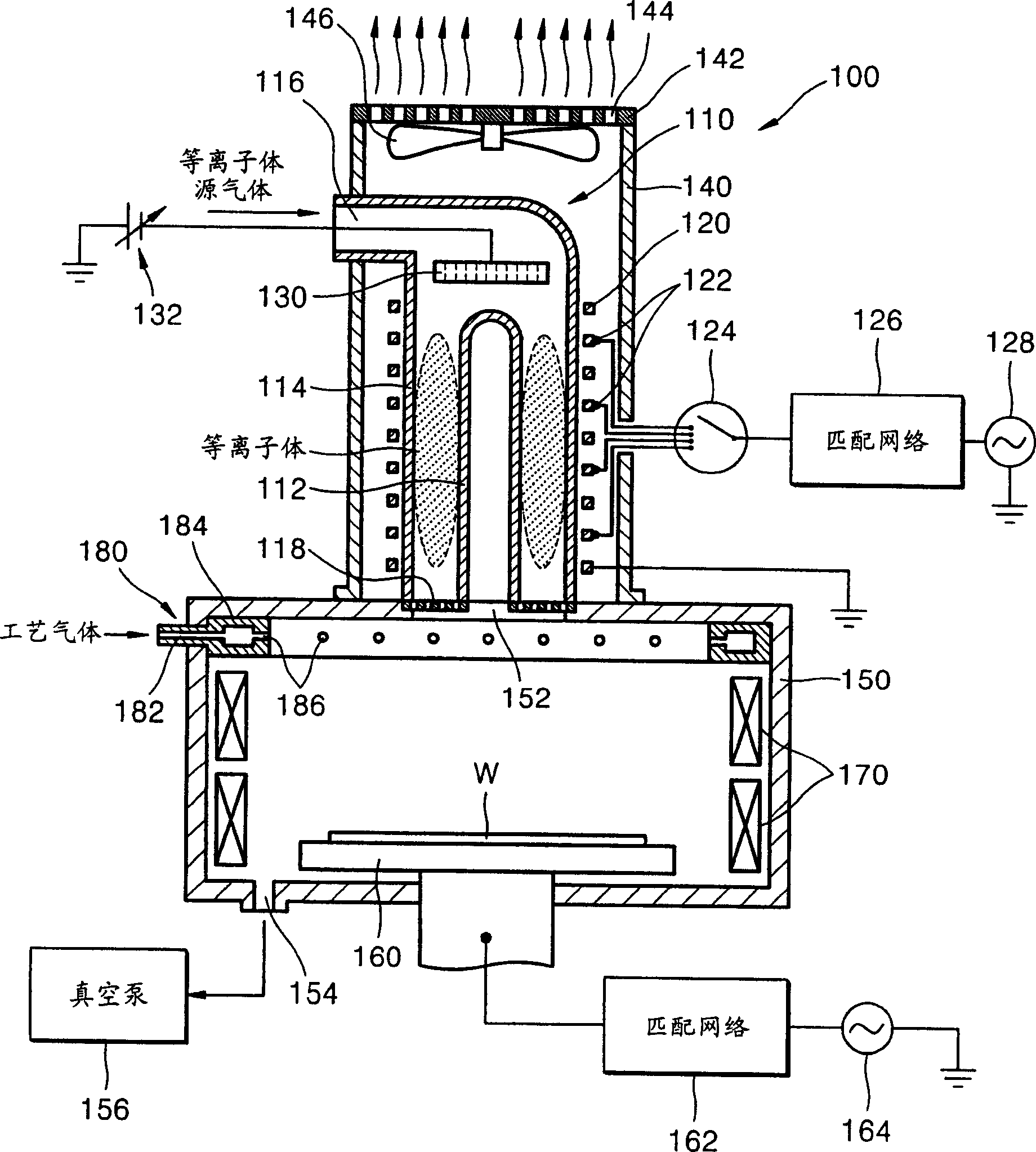
[0041] image 3 is a vertical cross-sectional view of a spiral resonator plasma processing apparatus according to a preferred embodiment of the present invention, Figure 4 yes image 3 A partially cut-away perspective view of the dielectric tube, control electrode, helical coil, and plasma distributor is shown.

[0042] refer to image 3 and 4 , the spiral resonator plasma processing apparatus according to the present invention is a semiconductor processing apparatus for performing fine processing by means of plasma generated by a spiral resonator 100, such as etching a substrate surface, or depositing a predetermined material on a substrate layer. The substrate loaded in the processing chamber 15...


PUM


Abstract

The invention discloses a spiral resonator plasma processing equipment. The plasma processing apparatus includes: a processing chamber having a substrate holder supporting a substrate to be processed; a dielectric tube disposed on the processing chamber so as to communicate with an interior space of the processing chamber; a helical coil wound around the outer tube of the dielectric tube; and an RF power supply that supplies RF power to the helical coil. The dielectric tube is in the form of a double tube, including an inner tube and an outer tube. A plasma source gas inlet is arranged in the outer tube to supply the plasma source gas into the space between the inner tube and the outer tube. A control electrode is arranged in the dielectric tube to control the plasma potential. This plasma processing apparatus provides a uniform plasma density distribution along the radial direction of the wafer and facilitates control of the plasma potential within the processing chamber.

Description

technical field [0001] The present invention relates to a plasma processing apparatus, and more particularly, to a helix resonator type plasma processing apparatus using a helix coil. Background technique [0002] Currently, plasma sources are widely used in the semiconductor industry to process fine semiconductor devices or flat display panels. That is, plasma sources are increasingly becoming indispensable in etching thin films or depositing predetermined thin material films on wafer surfaces for manufacturing semiconductor devices or depositing predetermined thin material films on substrates for manufacturing flat panel displays such as LCDs Tool of. Thus, the development of equipment for handling plasma sources has become a core requirement of the semiconductor industry. [0003] In recent years, with the rapid development of semiconductor technology, the integration density of semiconductor devices has been rapidly increased. Also, in order to improve processing effi...

Claims


Application Information

Patent Timeline
Patent Type & Authority Applications(China)
IPC IPC(8): H05H1/46H01J7/24H01J37/32H01L21/00H01L21/205H01L21/3065H05H1/00
CPCH01J37/321H01J37/3211H01J37/32697H01L21/00
Inventor 金大一马东俊金国闰崔圣圭
Owner SAMSUNG ELECTRONICS CO LTD
Why Eureka
Try Eureka