Plasma etching device

An etching device and plasma technology, applied in the direction of discharge tubes, electrical components, circuits, etc., can solve problems such as uneven etching of wafers, achieve the effects of weakening coherence, uniform electric field distribution, and eliminating standing wave effects

Active Publication Date: 2014-01-15
SEMICON MFG INT (SHANGHAI) CORP
View PDF8 Cites 8 Cited by
  • Summary
  • Abstract
  • Description
  • Claims
  • Application Information

AI Technical Summary

Problems solved by technology

[0009] The problem solved by the present invention is that the plasma etching device in the prior art will produce the problem of uneven etching of the wafer during the etching process

Method used


Image

  • Plasma etching device
  • Plasma etching device
  • Plasma etching device

Examples


no. 1 example

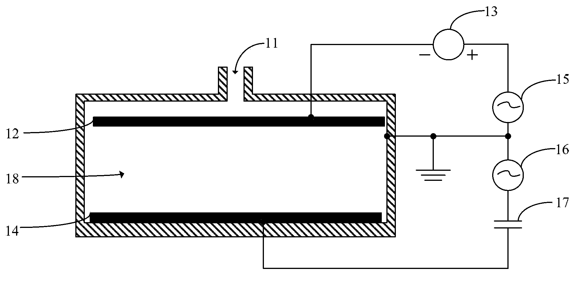
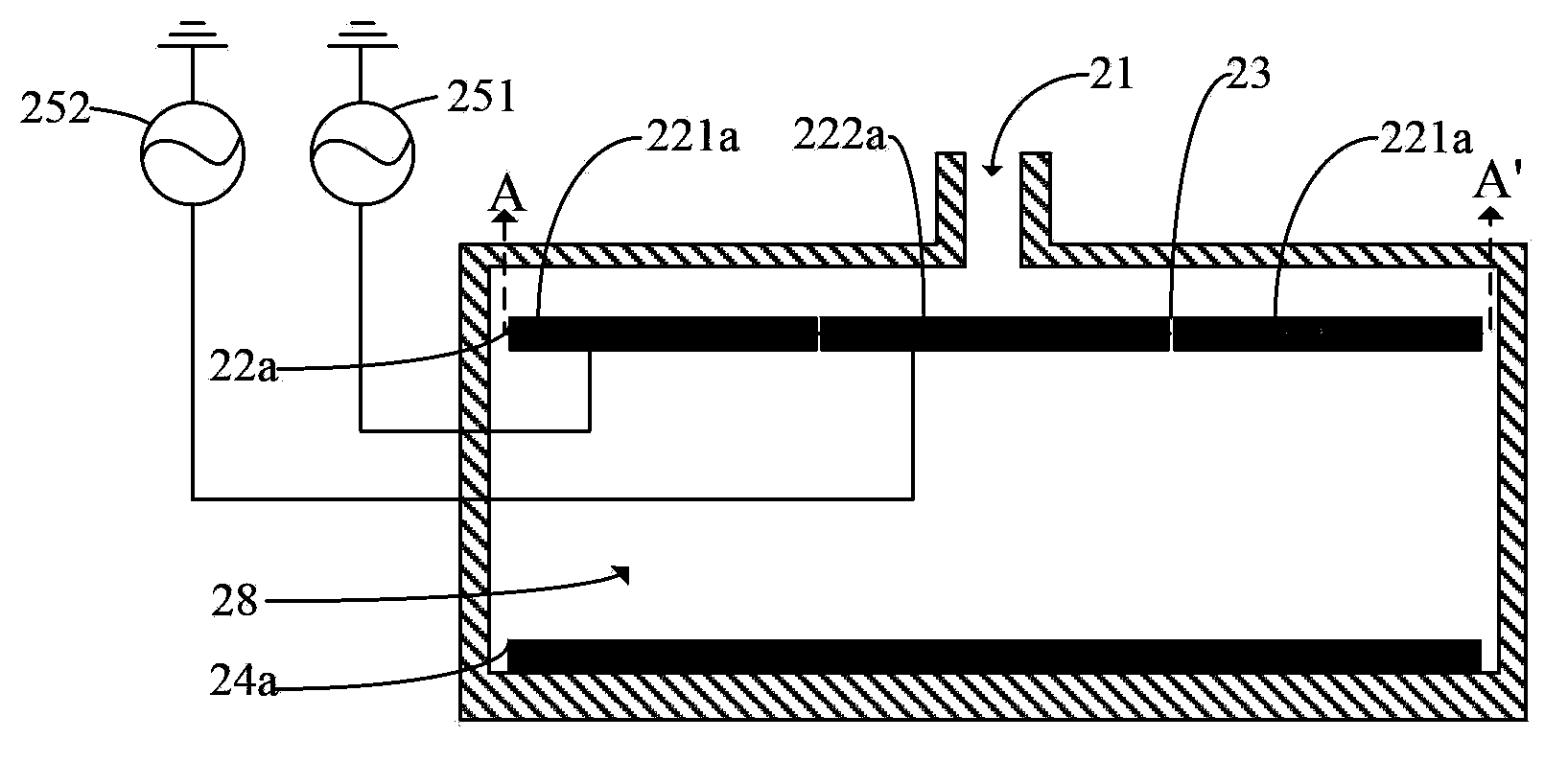
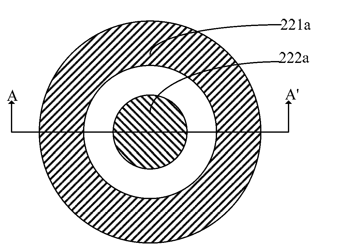
[0044] refer to figure 2 , in the first embodiment, the plasma etching device includes: a process chamber 28 having an opening 21; a first electrode 22a and a second electrode 24a located in the process chamber 28, and the first electrode is opposite to the second electrode Placement, the first electrode is positioned at the top of the process chamber, wherein the first electrode 22a includes a pole plate 221a and a pole plate 222a; an excitation radio frequency unit, the number of excitation radio frequency units is equal to the number of pole plates, and each pole plate is connected to each pole plate The excitation radio frequency units are electrically connected one to one, and the excitation radio frequency units are used to provide excitation energy to the etching gas in the process chamber through each plate of the first electrode. In this first embodiment, two excitation radio frequency units are included , are respectively the excitation radio frequency unit 251 elec...

no. 2 example

[0055] refer to Figure 6 , in the second embodiment, the plasma etching device includes: a low-frequency capacitively coupled RF generator 261 and a DC power supply 262 electrically connected to the second electrode 24b, and the other end of the low-frequency capacitively coupled RF generator 261 and the DC power supply 262 grounded. Among them, the low-frequency capacitively coupled RF generator 261 forms a low-frequency oscillating electric field in the process chamber 28 by providing a bias voltage to the second electrode 24b; form a stable electric field. The low-frequency oscillating electric field and stable electric field propagating in the process chamber 28 can change the movement direction of electrons in the plasma in the process chamber 28, thereby changing the propagation direction of part of the electromagnetic waves generated by the high-speed movement of electrons in the process chamber 28, This can further reduce or even eliminate standing wave effects. Th...

no. 3 example

[0059] refer to Figure 7 , in the third embodiment, the second electrode 24c includes two pole plates, namely pole plate 241c and pole plate 242c, wherein, pole plate 241c is electrically connected with one end of the low-frequency capacitive coupling RF generator 261, and the low-frequency capacitive coupling The other end of the RF generator 261 is grounded; one end of the plate 242c is electrically connected to the DC power supply 262, and the other end of the DC power supply 262 is grounded.

[0060] In the third embodiment, the shape and positional relationship of the two plates included in the second electrode 24c are the same as those of the two plates of the first electrode in the first embodiment, and will not be described in detail here. In addition, the number of pole plates of the second electrode is not limited to two pole plates, and may be three or more including three. The number of pole plates of the first electrode is the same as the number of pole plates o...


PUM


Abstract

The invention relates to a plasma etching device comprising a technological cavity, a first electrode, a second electrode, and excitation radio frequency units. The first electrode and the second electrode are arranged in the technological cavity and are opposite to each other; and the first electrode includes at least two polar plates. The number of the excitation radio frequency units are identical with that of the polar plates and all the polar plates and all the excitation radio frequency units are in one-to-one electrical connection; and the excitation radio frequency units are used for providing excitation energy for etching gas in the technological cavity by all the polar plates of the first electrode. On the basis of the difference of output frequencies of all the excitation radio frequency units, phase differences between emission radio frequencies of all the excitation radio frequency units, or differences of frequencies and phases of the emission radio frequencies, a standing wave occurrence caused by coherence due to opposite transmission of electromagnetic waves in the technological cavity can be avoided by using the plasma etching device. Therefore, a standing wave effect in the technological cavity can be weakened or even eliminated; the plasma with the high-density uniformity can be obtained; and uniform etching on the large-size wafer can be realized.

Description

technical field [0001] The invention relates to the field of semiconductors, in particular to a plasma etching device. Background technique [0002] In the prior art, as a commonly used wafer etching process, plasma etching uses an appropriate gas as the etching gas, and excites the etching process through an energy source, such as a high-frequency capacitively coupled RF generator or a high-frequency inductively coupled RF generator. The etchant gas is used to form plasma, and then the plasma is used to etch the area without the photolithography mask to form the required pattern in the wafer. [0003] In the prior art, refer to figure 1 , the plasma etching device mainly includes: a process chamber 18 with an opening 11, which is used for the input of etching gas; an upper plate 12 and a lower plate 14 located in the process chamber 18; a DC power supply 13, one end of which is connected to the The upper plate 12 is connected, and the other end is connected to the high-fr...

Claims


Application Information

Patent Timeline
Patent Type & Authority Applications(China)
IPC IPC(8): H01J37/32
Inventor 王冬江符雅丽张海洋
Owner SEMICON MFG INT (SHANGHAI) CORP
Why Eureka
Try Eureka