Semi-penetrating and semi-reflecting liquid-crystal displaying panel, pixel structure and manufacture thereof

A semi-transmissive, semi-reflective, liquid crystal display panel technology, applied in semiconductor/solid-state device manufacturing, transistors, static indicators, etc., can solve the problems of increasing backlight, energy consumption, etc., to improve light reflectivity, increase brightness, Enhance the effect of the refraction effect

Active Publication Date: 2005-07-27
AU OPTRONICS CORP
View PDF0 Cites 2 Cited by
  • Summary
  • Abstract
  • Description
  • Claims
  • Application Information

AI Technical Summary

Problems solved by technology

Once the aperture ratio of the penetrating part of the pixel is insufficient, in order to maintain the qual

Method used


Image

  • Semi-penetrating and semi-reflecting liquid-crystal displaying panel, pixel structure and manufacture thereof
  • Semi-penetrating and semi-reflecting liquid-crystal displaying panel, pixel structure and manufacture thereof
  • Semi-penetrating and semi-reflecting liquid-crystal displaying panel, pixel structure and manufacture thereof

Examples


no. 1 example

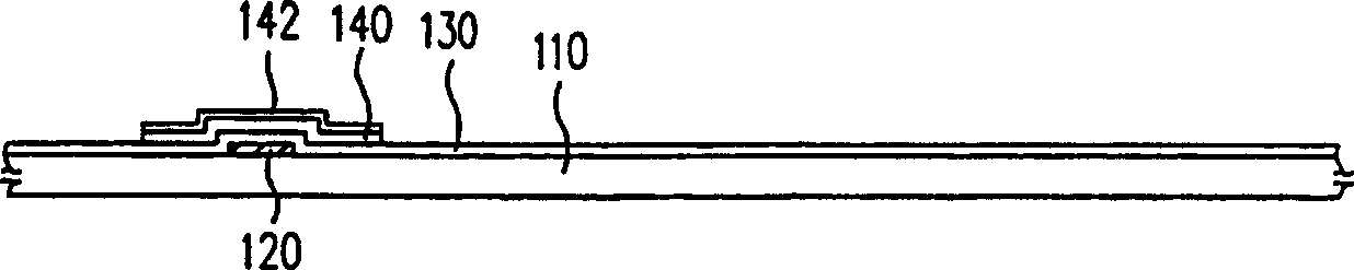
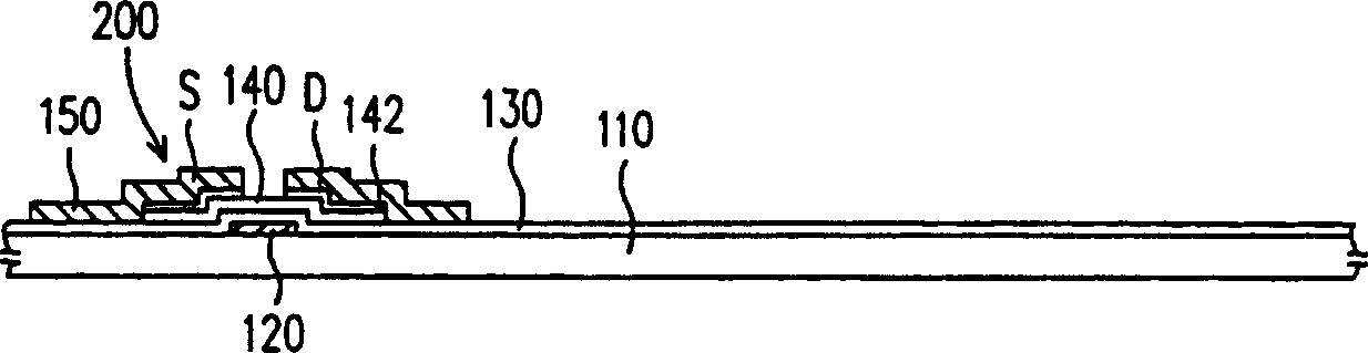
[0062] 1A-1F show the cross section of the manufacturing process of the transflective pixel structure according to the first embodiment of the present invention. figure 2 A schematic top view of the transflective pixel structure according to the first embodiment of the present invention is shown. Please refer to Figure 1A and figure 2 First, a scanning wiring 190 and a grid 120 are formed on a substrate 110, wherein the material of the substrate 110 is, for example, a glass substrate, a plastic substrate or other materials, and the material of the scanning wiring and the grid 120 is, for example, Chromium (Cr), tantalum (Ta) or other metal materials. After that, a gate insulating layer 130 is formed to cover the scan wiring 190 and the gate electrode 120 . Wherein, the material of the gate insulating layer 130 is, for example, silicon oxide, silicon nitride or other dielectric materials. Next, a channel layer 140 is formed to cover the gate insulating layer 130 , wherei...

no. 2 example

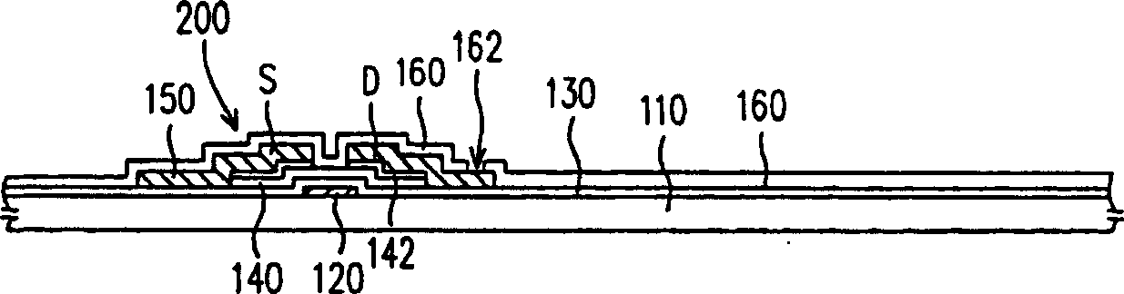
[0071] Figure 3A~Figure 3D A cross-sectional schematic diagram of the manufacturing process of the pixel structure according to the second embodiment of the present invention is shown. Since the manufacturing process of this embodiment is similar to that of the first embodiment, the reference numbers of this embodiment follow those of the first embodiment. Please refer to Figure 3A , first carry out the first embodiment Figure 1A to Figure 1B The process described above, and after the protective layer 160 is formed on the substrate 110, a plurality of raised patterns 164 (bumps) are formed on the protective layer 160 at the reflective area where the pixel electrode is scheduled to be formed, and the material thereof is, for example, organic resin (organicresin) or Is other organic materials (organic material). Wherein, the method of forming the protruding pattern 164 is, for example, firstly forming an organic material on the above-mentioned formed structure, and then pa...


PUM

PropertyMeasurementUnit
Thicknessaaaaaaaaaa
Diameteraaaaaaaaaa
Thicknessaaaaaaaaaa

Abstract

A preparing method includes disposing scan and data wiring on base plate for defining out a picture element region, disposing film transistor (FT) in the picture element region (PER) and connecting it to scan and data wiring, disposing picture element electrode (PEE) in PER corresponding to FT as PEE connected with FT and PEE having a reflection region and penetrating region, covering organic material (OM) on FT and PEE as multiple refractive patterns set on OM layer above penetrating region of PEE.

Description

technical field [0001] The present invention relates to a liquid crystal display panel and its pixel structure and manufacturing method, in particular to a semi-transmissive and semi-reflective liquid crystal display panel and its pixel structure and manufacturing method. Background technique [0002] With the rapid development of the information industry in recent years, the application of display technology, especially in portable information products, has been directed towards miniaturization, thinning, high brightness, low energy consumption, and high-quality full-color image output. step forward. [0003] In order to meet the needs of the above-mentioned portable information products, a reflective liquid crystal display technology has been proposed in the prior art. This technology uses a conductive material with the characteristic of reflecting light as the pixel electrode of the reflective liquid crystal display panel, and transmits incident light from the outside. T...

Claims


Application Information

Patent Timeline
IPC IPC(8): G02F1/133G02F1/136H01L21/027H01L29/786
Inventor 王净亦
Owner AU OPTRONICS CORP
Why Eureka
Try Eureka