Voltage controlled oscillator

A voltage-controlled oscillator and oscillation frequency technology, applied in power oscillators, automatic power control, pulse generation, etc., can solve the problems of oscillation frequency fluctuation, current value swing, cost increase, etc., and achieve low phase noise and reduced phase noise. Volatile, low-cost effects

Inactive Publication Date: 2005-07-27
PANASONIC CORP
View PDF0 Cites 15 Cited by
  • Summary
  • Abstract
  • Description
  • Claims
  • Application Information

AI Technical Summary

Problems solved by technology

Therefore, the chip size of the voltage controlled oscillator is increased, resulting in an increase in cost
[0021] In addition, in the conventional structure, a resistor is used instead of a current source transistor, so that, for example, when the power supply voltage changes, such as when operating a transmission circuit, the current value swings and the oscillation frequency fluctuates

Method used


Image

  • Voltage controlled oscillator
  • Voltage controlled oscillator
  • Voltage controlled oscillator

Examples


no. 1 example

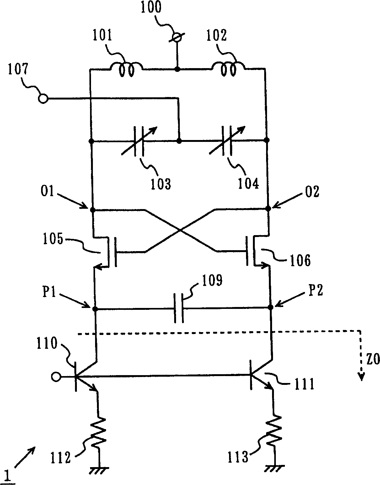
[0080] figure 1 It is a circuit diagram showing the structure of the voltage-controlled oscillator 1 according to the first embodiment of the present invention. exist figure 1The VCO 1 includes a power supply terminal 100, inductors 101 and 102, variable capacitance elements 103 and 104, oscillation transistors 105 and 106, a frequency control terminal 107, a coupling capacitor 109, current source transistors 110 and 111, and resistors 112 and 113. exist figure 1 , the bias circuit and the like are omitted.

[0081] The variable capacitance elements 103 and 104 utilize the gate capacitance of a variable capacitance diode or a field effect transistor (FET). The oscillation transistors 105 and 106 are field effect transistors (both referred to as "FETs" hereinafter). The coupling capacitor 109 is a capacitor having a predetermined capacitance value. Current source transistors 110 and 111 are bipolar transistors.

[0082] Inductors 101 and 102 are connected in series. The...

no. 2 example

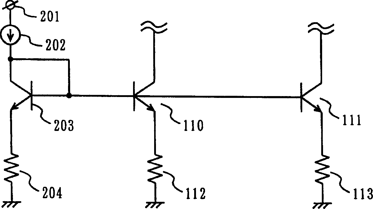
[0106] Figure 5 It is a circuit diagram showing the structure of the voltage-controlled oscillator 2 according to the second embodiment of the present invention. exist Figure 5 The VCO 2 includes a power supply terminal 100, inductors 101 and 102, variable capacitance elements 103 and 104, oscillation transistors 105 and 106, a frequency control terminal 107, a coupling capacitor 109, current source transistors 110 and 111, a resistor 112 and 113, and inductors 120 and 121. exist Figure 5 , the bias circuit and the like are omitted. exist Figure 5 , the same parts as those in the first embodiment have the same reference numerals and will not be described further.

[0107] In the first embodiment, the parasitic capacitance between the emitters and collectors of the current source transistors 110 and 111 reduces the impedance Z0 viewed from the terminals P1 and P2 to the current source side with respect to the higher oscillation frequency . For example, when the oscil...

no. 3 example

[0122] Figure 8 It is a circuit diagram showing the structure of the voltage-controlled oscillator 3 according to the third embodiment of the present invention. exist Figure 8 In the above, the voltage controlled oscillator 3 includes a power supply terminal 100, inductors 101 and 102, variable capacitance elements 103 and 104, oscillation transistors 105 and 106, a frequency control terminal 107, a coupling capacitor 109, current source transistors 110 and 111, and inductors 132 and 106. 133. Figure 8 The bias circuit and the like are omitted. Figure 8 , the same parts as those in the first embodiment have the same reference numerals and will not be further described.

[0123] Inductors 132 and 133 are connected to the emitters of current source transistors 110 and 111 and grounded. The impedances of the inductors 132 and 133 can suppress the signal at the two terminals of the coupling capacitor 109 whose frequency is twice the oscillation frequency, which is similar ...


PUM


Abstract

The present invention provides a voltage controlled oscillator for changing an oscillating frequency in accordance an input control voltage, including a parallel resonant circuit, a negative resistance circuit connected in parallel to the parallel resonant circuit, a first capacitor connected in parallel to the negative resistance circuit, a first current source connected between one terminal of the first capacitor and the negative resistance circuit, and a second current source connected between the other terminal of the first capacitor and the negative resistance circuit. The capacitance value of the first capacitor is set to a value that suppresses a signal with a frequency twice the oscillating frequency at both the terminals of the first capacitor. Each of the first and the second current sources is constituted by a bipolar transistor.

Description

technical field [0001] The present invention relates to voltage controlled oscillators used in wireless communication devices and PLL circuits. In particular, the present invention relates to a voltage controlled oscillator capable of suppressing phase noise. Background technique [0002] Voltage-controlled oscillators are widely used as means for generating local oscillator signals for wireless communication devices. FIG. 19 is a circuit diagram showing the structure of a conventional voltage-controlled oscillator 900 . In FIG. 19, the voltage controlled oscillator includes a power supply terminal 910, inductors 911 and 912, variable capacitance elements 913 and 914, oscillation transistors 915 and 916, a frequency control terminal 917, and a current source transistor 930. Bias circuits and the like are omitted in FIG. 19 . [0003] In FIG. 19, inductances 911 and 912 and variable capacitance elements 913 and 914 constitute a parallel resonance circuit. The capacitance ...

Claims


Application Information

Patent Timeline
Patent Type & Authority Applications(China)
IPC IPC(8): H03K3/354
CPCH03K3/354
Inventor 滝波浩二築澤貴行足立寿史大原淳史
Owner PANASONIC CORP
Why Eureka
Try Eureka