
Semiconductor device

A semiconductor and equipment technology, applied in the field of semiconductor equipment, can solve the problem that transistors cannot be used as storage elements, and achieve the effect of improving diversity

Inactive Publication Date: 2005-07-27
矽利康创新有限公司
View PDF0 Cites 2 Cited by
  • Summary
  • Abstract
  • Description
  • Claims
  • Application Information

AI Technical Summary

Problems solved by technology

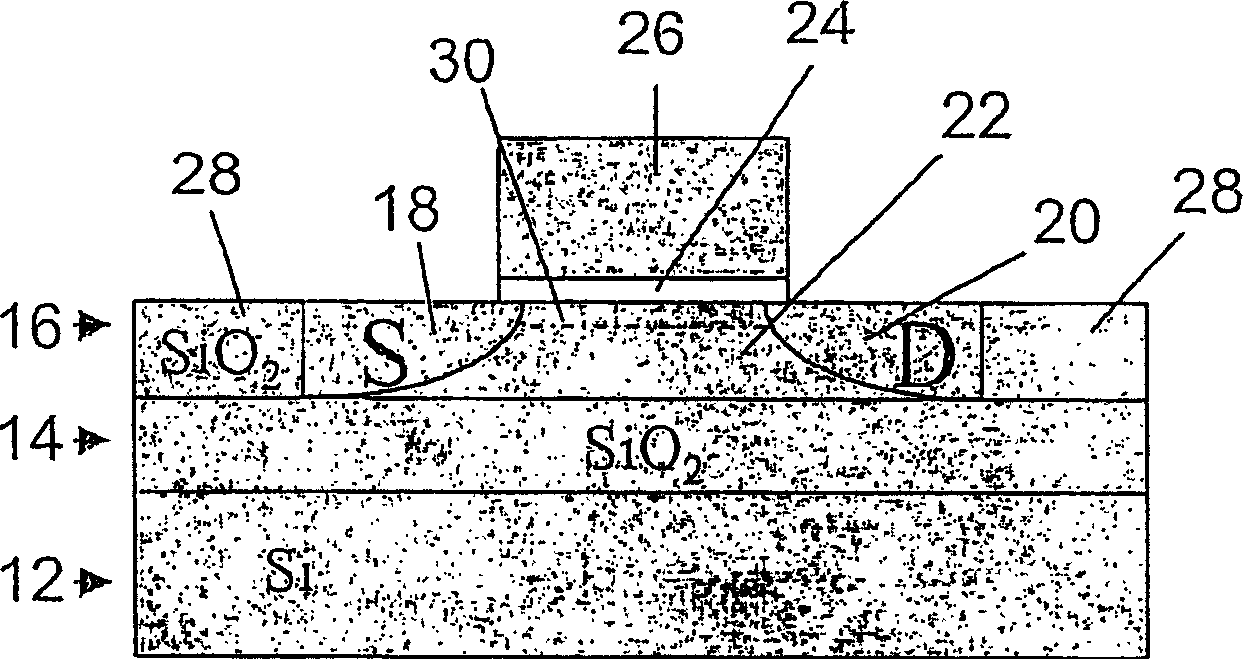
It is thus impossible to store charge in the body 22, and this type of transistor cannot therefore be used as a storage element.

Method used

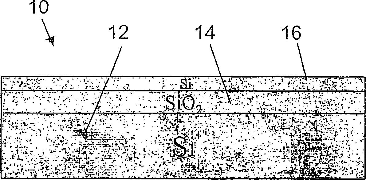

Image

  • Semiconductor device
  • Semiconductor device
  • Semiconductor device

Examples


Embodiment Construction

[0057] refer to Figure 6 , which shows a semiconductor device embodying the invention, Figure 6 Parts of the apparatus shown in Fig. 5a that are the same as those in Fig. 5a are indicated by the same reference numerals. An NMOS transistor is formed in a first semiconductor layer in the form of a silicon layer 16 and overlaid with an insulating layer 32 which is perforated to form windows which are filled with conductive material to form contact areas 34, 35, respectively It is connected to the source region 18 and the drain region 20. Contact areas 34, 35 are also connected to conductors 36, 37, respectively.

[0058] Figure 6 The NMOS transistor shown has a base layer 12 of n-type silicon with a second semiconductor layer in the form of a box-like region 38 of p-type silicon, which has a doping concentration higher than that of the body 22 but lower. The impurity concentration of the corresponding source 18 and drain 20. The box-shaped area 38 is connected to a conduc...


PUM


Abstract

A semiconductor device such as a DRAM memory device is disclosed. A substrate 12 of semiconductor material is provided with energy band modifying means in the form of a box region 38 and is covered by an insulating layer 14. A semiconductor layer 16 has source 18 and drain 20 regions formed therein to define bodies 22 of respective field effect transistors. The box region 38 is more heavily doped than the adjacent body 22, but less highly doped than the corresponding source 18 and drain 20, and modifies the valence and / or conduction band of the body 22 to increase the amount of electrical charge which can be stored in the body 22.

Description

technical field [0001] The present invention relates to a semiconductor device, in particular but not exclusively to a semiconductor storage device such as a semiconductor memory, and to a substrate for manufacturing such a device. Background technique [0002] The document of International Patent No. PCT / EP02 / 06495 discloses a DRAM device (Dynamic Random Access Memory) comprising a matrix of memory cells, each cell consisting of a field effect transistor. Charge is generated and stored within the bulk of each transistor by applying appropriate voltage pulses between the gate and drain, and between the source and drain of each transistor. The presence or absence of charge represents the "1" and "0" states of a binary data bit, respectively. Memory devices using SOI (Silicon Insulator) type field effect transistors are described in detail in "SOI technology: materials to VLSI", 2nd edition, Kluwer, Boston, 1997. [0003] The transistors used in this type of device are PD-SO...

Claims


Application Information

Patent Timeline
IPC IPC(8): H01L21/8242H01L27/108H01L27/12H01L29/739H01L29/786H01L29/788
CPCH01L29/7391H01L29/7881H01L29/7841H01L29/78648H01L27/10873G11C2211/4016H01L29/78645H01L27/108H01L29/78696H01L27/10802H01L27/1203H10B12/20H10B12/05H10B12/00
Inventor 皮埃尔·克里斯托夫·法赞塞尔格·奥霍宁
Owner 矽利康创新有限公司
Learn More