Optical technique for detecting buried defects in opaque films

A technology of detectors and optical equipment, applied in the direction of material analysis, measuring devices, scientific instruments, etc. by optical means, which can solve the problems of slow and expensive analysis

Inactive Publication Date: 2005-08-31
APPLIED MATERIALS INC +1
View PDF6 Cites 15 Cited by
  • Summary
  • Abstract
  • Description
  • Claims
  • Application Information

AI Technical Summary

Problems solved by technology

These analyzes are slow and expensive

Method used


Image

  • Optical technique for detecting buried defects in opaque films
  • Optical technique for detecting buried defects in opaque films
  • Optical technique for detecting buried defects in opaque films

Examples


Embodiment 1

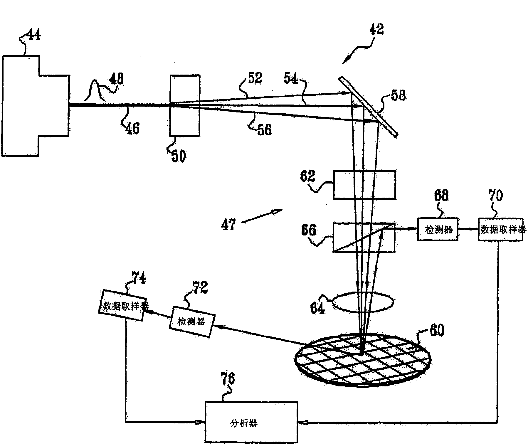
[0144] Now refer to figure 2 , which is a schematic diagram of an optical inspection system 42 constructed and operative in accordance with a disclosed embodiment of the present invention. figure 2 Several features are shown that are common to other embodiments disclosed below. Details of these common features will not be repeated for the sake of brevity.

[0145] A mode-locked laser source 44 emits a pulsed beam 46 of light (shown schematically as pulse 48). The laser source 44 can be a Vitesse mode-locked Ti:sapphire laser, which can generate 100×10 -15 second pulse, or a DPM-1000 DPSS mode-locked Nd:YVO laser, which can generate 3×10 -12 second pulse. Both laser sources are commercially available from Coherent, Santa Clara, CA, USA. In some embodiments, laser source 44 may generate a laser with a duration between 100×10 -15 seconds to 1×10 -9 pulses between seconds. Alternatively, a source of pulsed incoherent light may be used to generate the beam 46, except in e...

Embodiment 2

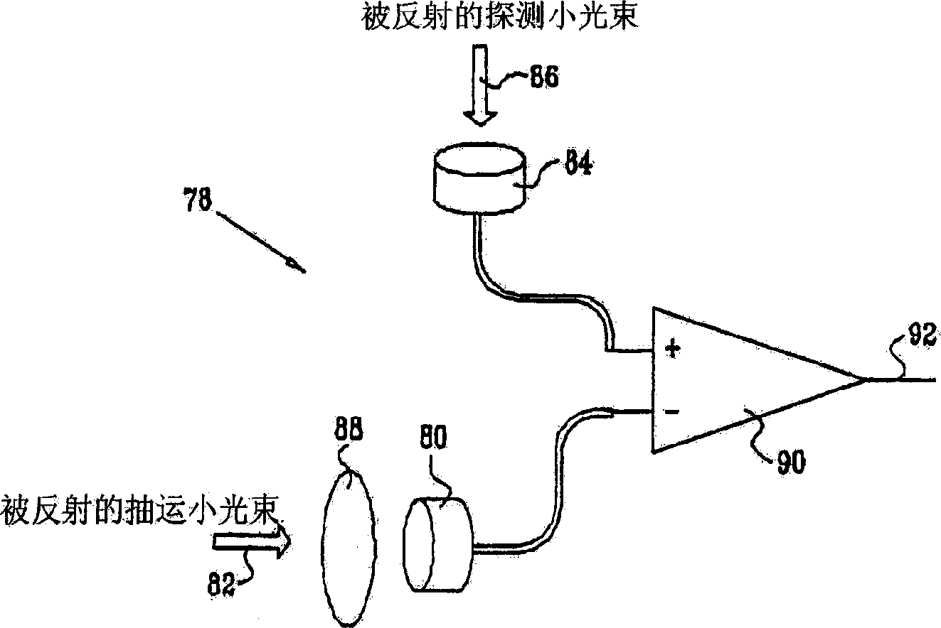
[0159] Now refer to Figure 4 , which is a schematic diagram of an optical inspection system 94 constructed and operative in accordance with another embodiment of the present invention. A mode-locked laser source 96 emits a variably polarized output beam 98 having a desired output intensity ratio, as will be described below. Alternatively, a pulsed incoherent light source may be used to generate the light beam 98, except for embodiments having a DIC configuration. Beam 98 is split by a polarizing beam splitter 100 into a pump beamlet 102 and a probe beamlet 104 . The ratio of the intensity of pump beamlet 102 to probe beamlet 104 can be adjusted by adjusting the polarity of beam 98 . The pump beamlet 102 enters a nonpolar beam splitter 106 , passes through the focusing lens 64 , and irradiates the substrate 60 . The pump beamlet 102 may impinge on the substrate 60 either vertically or obliquely. The probe beamlet 104 passes through a retroreflector 108 and is reflected by ...

Embodiment 3

[0162] Now refer to Figure 5 , which is a schematic diagram of an optical inspection system 114 constructed and operated in accordance with another embodiment of the present invention. Many of the system 114 are similar to the system 94 ( Figure 4 ) will not be repeated for the sake of brevity. In system 114, the pulse 48 undergoes harmonic oscillation to generate a set of pulsed probe beamlets that are all perfectly synchronized with the pump beamlet and are separated from each other by wavelength. The light beam 46 passes through a second harmonically oscillating (SHG) crystal 116 . Thus, an outgoing light beam 118 has two distinct, harmonically related frequency components. The beam 118 is split by a beam splitter 120 into a pumping beamlet 122 and a probing beamlet 124 , the probing beamlet 124 has a frequency which is the second harmonic of the pumping beamlet 122 . Alternatively, the pump beamlet 122 may be the second harmonic of the probe beamlet 124 . The probe ...


PUM


Abstract

A local area of a sample is focally heated to produce a transient physical deformation. The surface of the structure is optically monitored while the heated area cools to a baseline temperature by illuminating the heated region with one or more probe beams from time to time and detecting returning light. In some embodiments heat dissipation within the structure is correlated with change in optical reflectivity over time. In other embodiments, surface deformation of the structure is correlated with changes in light scattering from the surface. Following application of a pump pulse and no more than 3 probe pulses, a time varying returning light signal is compared with a corresponding returning light signal from a reference. An anomaly in the sample is indicated by a deviation between the two signals. First-degree exponential decay curves may be constructed from the signals, and their decay constants compared.

Description

technical field [0001] The present invention relates to the manufacture of semiconductor components. In particular, the invention relates to the detection of surface defects in heterogeneous structures, such as in multilayer integrated circuits. Background technique [0002] Semiconductor structures are inspected before, during and after the patterning process. Patterned metal film layers in integrated circuit components are typically produced using a damascene technique in which a pattern is etched into an insulating dielectric layer, followed by several standard deposition techniques, such as chemical Any of vapor deposition (CVD), physical vapor deposition (PVD), or electronic copper plating (ECP) is used to fill the pattern. During this process, defects can be created in or under the metal, such as air gaps, underfilling or underetching of dielectric layers, and other interface-related defects can be created. [0003] In general, these defects are not directly accessi...

Claims


Application Information

Patent Timeline
Patent Type & Authority Applications(China)
IPC IPC(8): G01N21/17G01N21/63G01N21/956
CPCG01N21/956G01N2201/104G01N21/171G01N21/636G01N2021/95676G01N2201/10
Inventor 丹尼尔·I·索梅
Owner APPLIED MATERIALS INC
Why Eureka
Try Eureka