
A packaging structure with a chip above a photosensitive element and electric packaging structure thereof

A photosensitive element and packaging structure technology, applied in the direction of electrical components, circuits, electric solid devices, etc., can solve the problems of limiting the integration degree of the electrical packaging structure 100 and occupying the carrying area of ​​the circuit substrate 110, so as to improve the integration degree and reduce the carrying area Effect

Inactive Publication Date: 2005-09-21
UNITED MICROELECTRONICS CORP
View PDF0 Cites 0 Cited by
  • Summary
  • Abstract
  • Description
  • Claims
  • Application Information

AI Technical Summary

Problems solved by technology

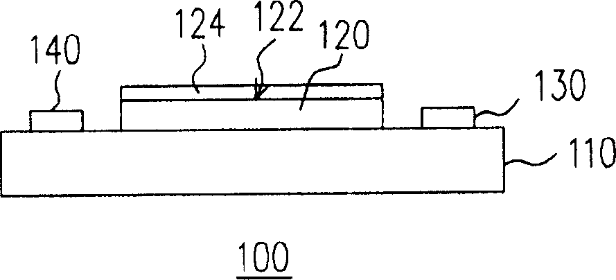
[0005] It should be noted that in the existing packaging technology, the image processing chip 130 and the non-volatile memory 140 are arranged on the upper surface or the lower surface of the circuit substrate 110, and are electrically connected with the circuit substrate 110. However, the image processing chip 130 and the non-volatile memory The volatile memory 140 will occupy the load-carrying area of ​​the circuit substrate 110, so that the circuit substrate 110 cannot be miniaturized, thereby limiting the integration of the electrical package structure 100

Method used


Image

  • A packaging structure with a chip above a photosensitive element and electric packaging structure thereof
  • A packaging structure with a chip above a photosensitive element and electric packaging structure thereof
  • A packaging structure with a chip above a photosensitive element and electric packaging structure thereof

Examples


Embodiment Construction

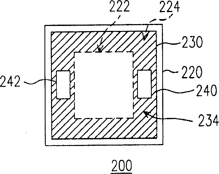
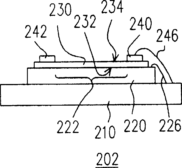
[0037] Please refer to figure 2 , which shows a top view of a packaging structure of a chip on a photosensitive element according to a preferred embodiment of the present invention. The packaging structure 200 mainly includes a photosensitive element 220 , a transparent plate 230 and a chip 240 . The photosensitive element 220 has a photosensitive area (inside the virtual frame) 222 and a non-photosensitive area (hatched area) 224, and the light-transmitting plate 230 is disposed on the photosensitive element 220 and covers the photosensitive area 222 and the non-photosensitive area 224 . In addition, the chip 240 is disposed on the surface 234 of the light-transmitting plate 230 , and the position of the chip 240 is above the non-photosensitive region 224 , so as to form a packaging structure 200 in which the chip 240 is stacked on the photosensitive element 220 .

[0038] In this embodiment, the photosensitive element 220 is, for example, a CCD image sensing element or a ...


PUM


Abstract

A package structure of chip on light sensitive device containing a light sensitive device, a light transparent board and a chip, wherein the light sensitive device having a light sensing area and a non light sensing area, the light transparent board having a first surface and second surface and located on light sensitive device, the first surface covering on light sensing area and non light sensing area, the chip located the second surface and above the non light sensing area.

Description

technical field [0001] The invention relates to a packaging structure, in particular to a packaging structure of a chip on a photosensitive element and an electrical packaging structure thereof. Background technique [0002] Charge Coupled Device (CCD) is the most commonly used image sensing element ( image sensor) one. However, the charge-coupled device also has problems such as high price due to special manufacturing process, high power consumption (Power Dissipation) due to high voltage operation of the driving circuit, and inability to perform random access (Random Access). [0003] The Complementary Metal Oxide Semiconductor (COMS) image sensing element has the characteristics of high quantum efficiency (QuantumEfficiency), low read noise (Read Noise), high dynamic range and random access, and is fully compatible with the CMOS manufacturing process, so it can be easily It can be easily integrated with other control circuits, analog-to-digital circuits (A / D Converter),...

Claims


Application Information

Patent Timeline
Patent Type & Authority Applications(China)
IPC IPC(8): H01L23/00H01L27/14H01L31/0203
CPCH01L2224/48091
Inventor 孙正光郑光志李光兴
Owner UNITED MICROELECTRONICS CORP
Learn More