Semiconductor device including bipolar junction transistor with protected emitter-base junction

A technology of bipolar junction transistors and semiconductors, applied in semiconductor devices, semiconductor/solid-state device manufacturing, transistors, etc., can solve the problems of reduced current amplification factor and increased leakage current

Inactive Publication Date: 2005-10-05
YAMAHA CORP
View PDF1 Cites 8 Cited by
  • Summary
  • Abstract
  • Description
  • Claims
  • Application Information

AI Technical Summary

Problems solved by technology

Therefore, when Figure 19 When the emitter region 13 is formed in the surface layer of the active base region 6 shown in , the leakage current at the pn junction between the emitter region 13 and the base region 6 increases, and the current amplification factor h FE reduce

Method used


Image

  • Semiconductor device including bipolar junction transistor with protected emitter-base junction
  • Semiconductor device including bipolar junction transistor with protected emitter-base junction
  • Semiconductor device including bipolar junction transistor with protected emitter-base junction

Examples


Embodiment Construction

[0055] Before describing the examples, preliminary studies by the present inventors will be described.

[0056] Figure 23 An example of a bipolar transistor fabricated by the present inventors in the course of research is shown. In this example, the number of steps is reduced.

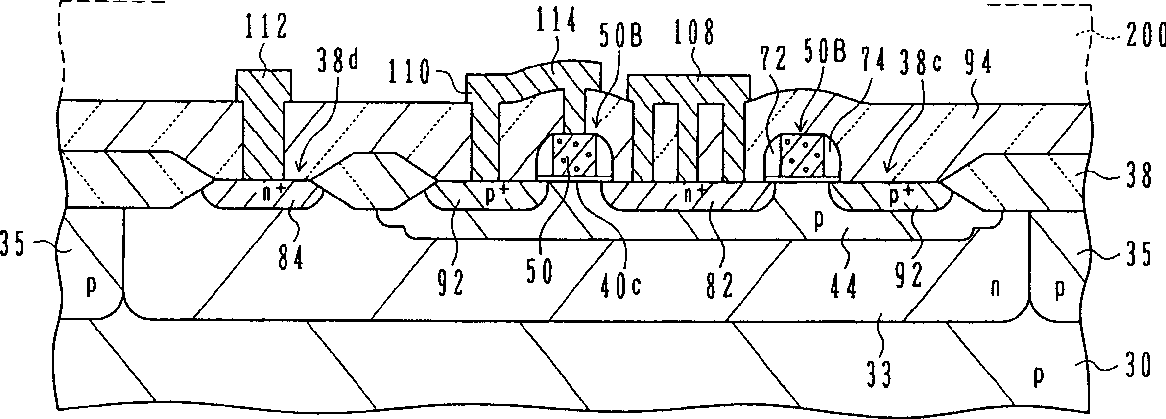
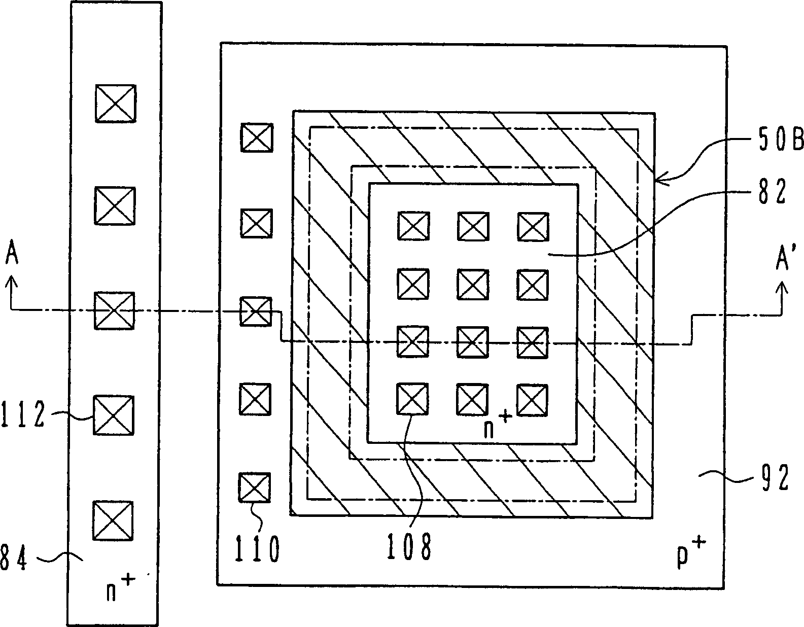
[0057] On one main surface layer of p-type silicon substrate 20, n-type collector region 21 and p-type isolation region 22 are formed. The n-type region 21 is formed by using an ion implantation process to form an n-type well of a p-channel MOS transistor in the CMOS transistor region. The p-type region 22 surrounding the n-type region 21 is formed by using an ion implantation process to form a p-type well of an n-channel MOS transistor in the CMOS transistor region.

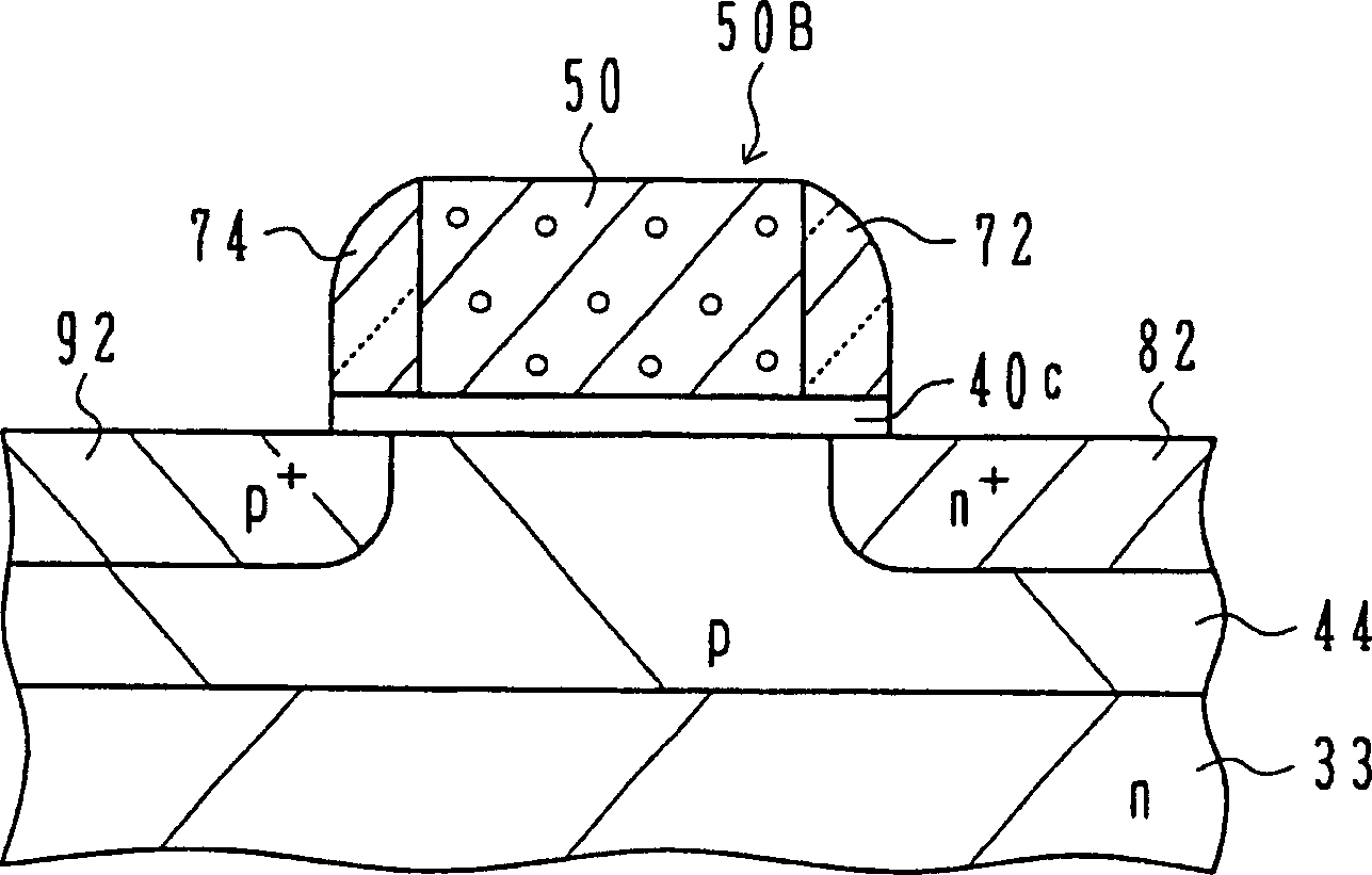
[0058] On the surface of the substrate 20 is formed a field oxide film 23 having emitter / base holes 23a and collector contact holes 23c. The oxide film 23 is formed by using a selective oxidation process for forming a field oxide fi...


PUM


Abstract

A method of manufacturing a CMOS-BJT semiconductor device comprises the steps of: forming a collector region of a first conductivity type and a first well of the first conductivity type, simultaneously in a semiconductor substrate; forming a second well of a second conductivity type opposite to said first conductivity type, in the semiconductor substrate; forming a base region of the second conductivity type in the collector region; forming first and second insulated gate structure on said first and second wells, and a junction protection structure having same constituent elements as said insulated gate structures on said base region; and forming second source / drain regions of the first conductivity type in said second well, and an emitter region of the first conductivity type in the base region, simultaneously, with an emitter-base junction reaching the principal surface below said junction protection structure.

Description

technical field [0001] The present invention relates to a semiconductor device and a manufacturing method thereof, in particular, the present invention relates to a semiconductor device including a complementary MOS (CMOS) transistor and a bipolar junction transistor (BJT) and a manufacturing method thereof. Background technique [0002] Figure 13-22 The fabrication method shown in is a conventional fabrication method for bipolar junction transistors (for example, refer to Japanese Patent Laid-Open No. SHO-62-86752, which is incorporated herein by reference). [0003] exist Figure 13 In the method shown in , in a p-type silicon substrate 1 having a main surface, an n-type collector region 2 is formed from the main surface down into the substrate. The n-type collector region 2 is formed by the same process as forming the n-type well of the p-channel MOS transistor in the CMOS transistor region. After forming field oxide film 3 having element aperture 3a corresponding to p...

Claims


Application Information

Patent Timeline
Patent Type & Authority Applications(China)
IPC IPC(8): H01L21/331H01L21/8222H01L21/8248H01L21/28H01L21/8249H01L27/01H01L27/06H01L29/417H01L29/423H01L29/49H01L29/72H01L29/732
CPCH01L21/8249H01L27/0623H01L29/66272H01L29/7322H01L29/72
Inventor 神谷孝行密冈久二彦
Owner YAMAHA CORP
Why Eureka
Try Eureka