Extracting wiring parasitics for filtered interconnections in an integrated circuit

A technology of integrated circuits and parasitic resistance, which is applied in the field of electronic design automation and can solve problems such as a large amount of memory and processing power

Inactive Publication Date: 2005-10-05
GLOBALFOUNDRIES INC
View PDF0 Cites 7 Cited by
  • Summary
  • Abstract
  • Description
  • Claims
  • Application Information

AI Technical Summary

Problems solved by technology

While these EDA vendors may have developed software tools that perform RC extractions more accurately, these software tools requ

Method used


Image

  • Extracting wiring parasitics for filtered interconnections in an integrated circuit
  • Extracting wiring parasitics for filtered interconnections in an integrated circuit
  • Extracting wiring parasitics for filtered interconnections in an integrated circuit

Examples


Embodiment Construction

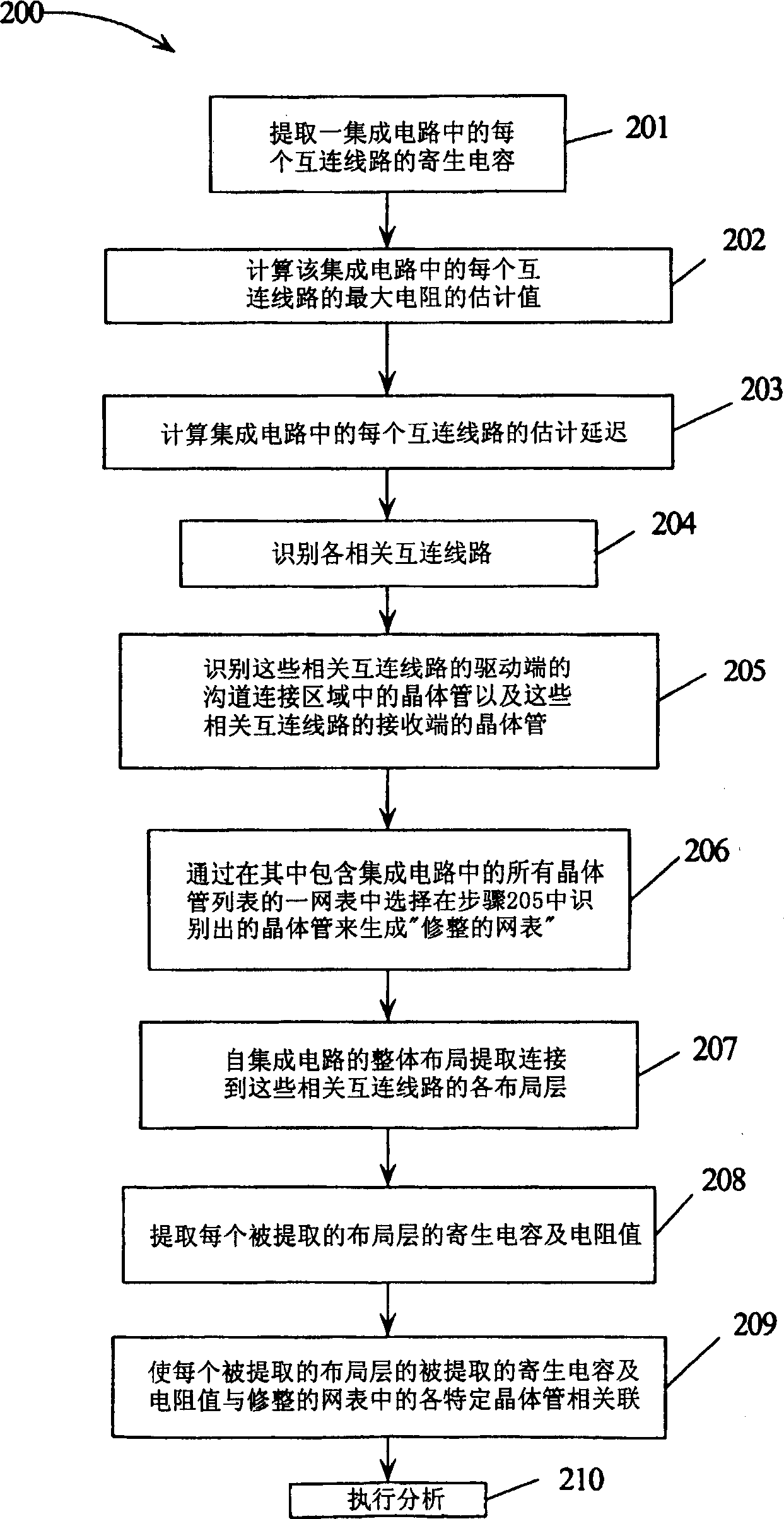
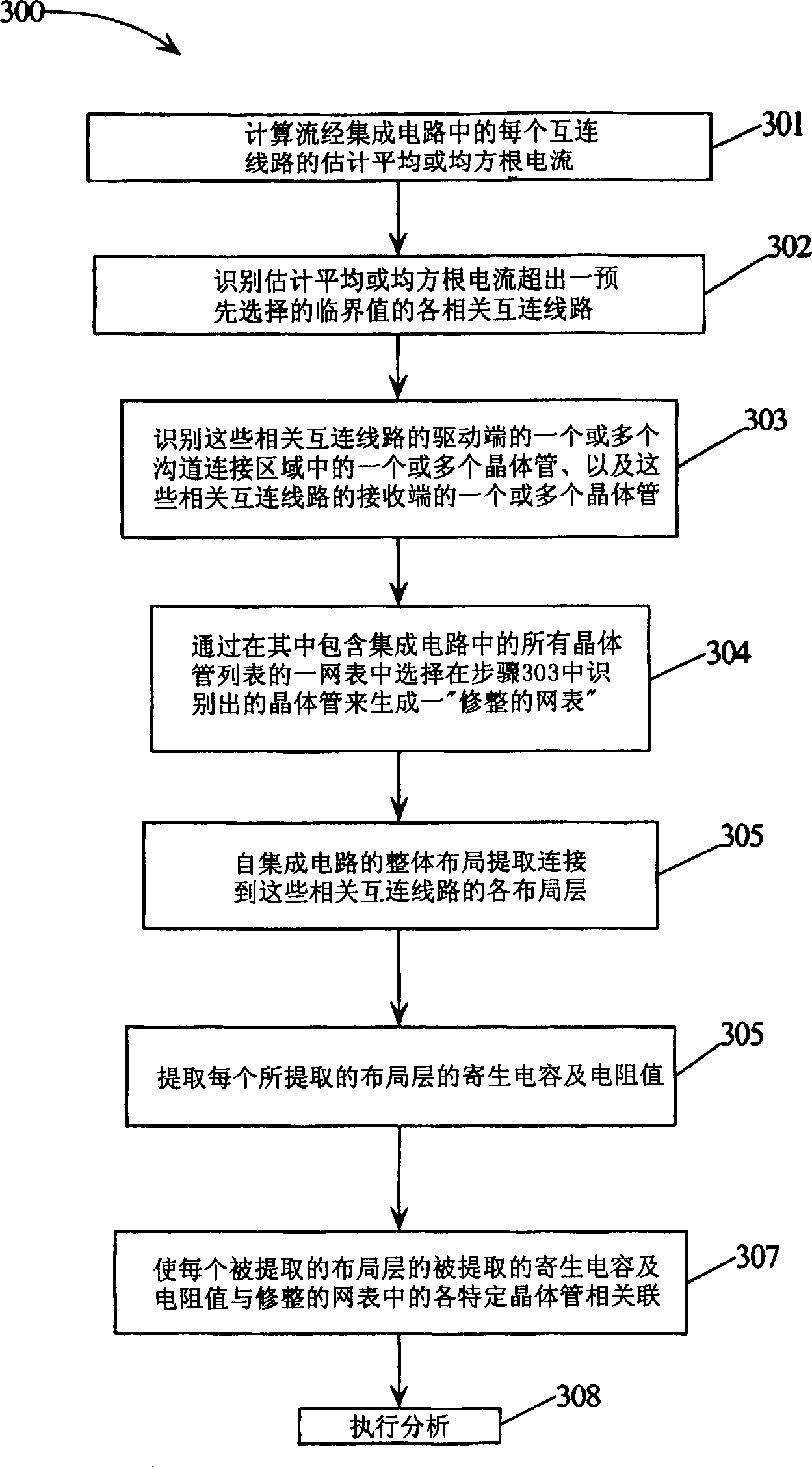
[0015] Please note that although extraction of parasitic resistance and capacitance values ​​to perform a delay and an electromigration analysis will be described below, the principles of the invention outlined below can be applied to applications such as power line net voltage drop analysis, clock network analysis, coupling Analysis and other types of analysis. Note also that one with ordinary knowledge in the art can apply the principles of the present invention to these types of analyses. Note also that embodiments that perform such analysis would still be within the scope of the present invention. Note also that for ease of reading, parasitic capacitance or parasitic resistance may be simply referred to as "capacitance" or "resistance", respectively.

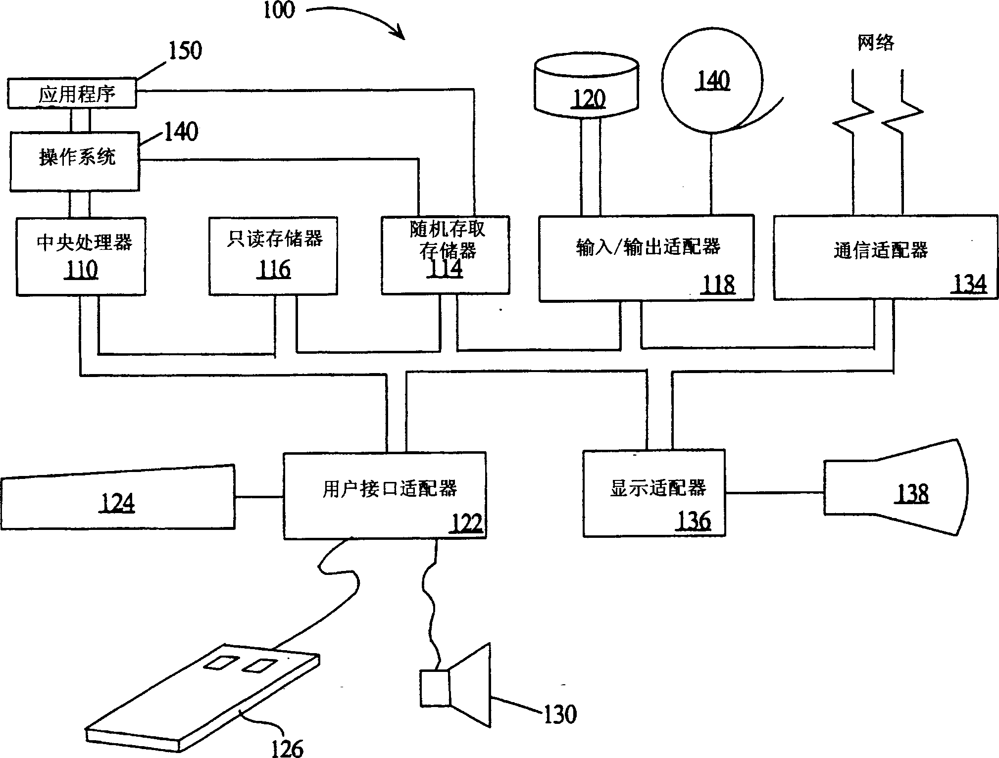
[0016] figure 1 - The hardware configuration of the computer system

[0017] figure 1 A typical hardware configuration of computer system 100, such as a workstation, is identified, representing a hardware environment in ...


PUM


Abstract

A method (200), system (100) and computer program product for extracting parasitic resistance and capacitance values to simulate performance values to simulate performance of an integrated circuit. A selected number of interconnections in an integrated circuit may be identified (204) ('interconnections of interest'). A netlist containing a list of the transistors in the integrated circuit may be pruned by selecting those transistors in the netlist that are in the channel connected regions on the driving side of the interconnections of interest and those on the receiving side of the interconnections of interest (205, 206). Parasitic resistance and capacitance values for layout layers connected to the interconnections of interest may be extracted (208). These extracted parasitic resistance and capacitance values may be associated with the transistors connected to those layout layers in the pruned netlist (209). By extracting parasitic resistance and capacitance values as describe above, less compute-intensive RC extractions may be made thereby using less memory and processing power.

Description

technical field [0001] The present invention relates to the field of electronic design automation, and more particularly to a method and system for extracting parasitic resistance and capacitance of selected interconnections in an integrated circuit using less memory and processing power than the prior art. Background technique [0002] The field commonly referred to as Electronic Design Automation (EDA) has evolved to handle the demanding and complex design of semiconductor integrated circuits. EDA means the use of computers to design and simulate the performance of electronic circuits on integrated circuits, commonly referred to as "chips." Computers are well suited for performing the tasks associated with designing programs because they can be programmed to reduce, or break down, large and complex circuits into simpler functional units. [0003] After the circuitry of a semiconductor chip has been designed and physically laid out, the operation of the integrated circuit ...

Claims


Application Information

Patent Timeline
IPC IPC(8): G06F17/50H01L21/82
CPCG06F17/5036G06F17/5081G06F30/367G06F30/398
Inventor M·S·夏尔马D·M·纽马克T·辛格J·A·贝尔
Owner GLOBALFOUNDRIES INC
Why Eureka
Try Eureka