Multi layer gridding detector of chip, and method for anti attack

A multi-layer grid and detector technology, applied in the direction of instruments, electric solid devices, semiconductor devices, etc., can solve problems such as attacks, technical defects, and inability to effectively protect chips, and achieve the effect of achieving protection and increasing difficulty

Active Publication Date: 2005-11-16
SHENZHEN SINOSUN TECH
View PDF0 Cites 7 Cited by
  • Summary
  • Abstract
  • Description
  • Claims
  • Application Information

AI Technical Summary

Problems solved by technology

[0008] However, in the prior art, there has been a technical means of using laser cutting to break through the metal grid for this kind of metal grid. Therefore, for particularly important core information, the use of laser cutting technology can destroy the metal grid of each layer without causing damage. Destroy the internal structure of the chip, and then use the above technical means to carry out a successful attack
[0009] Therefore, the chip technology of the prior art still cannot effectively protect the chip that stores important core data, and it has technical defects, which need to be improved and developed.

Method used


Image

  • Multi layer gridding detector of chip, and method for anti attack
  • Multi layer gridding detector of chip, and method for anti attack
  • Multi layer gridding detector of chip, and method for anti attack

Examples


Embodiment Construction

[0030] Various preferred embodiments of the present invention will be described in detail below in conjunction with the accompanying drawings.

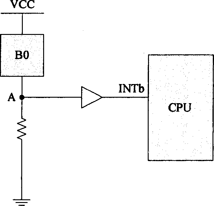
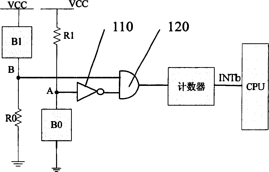
[0031] The chip multi-layer grid detector and its anti-attack method of the present invention is a multi-layer grid detector technology that prevents laser cutting attacks, which can be used in integrated circuit design for program and data storage Protect the area to prevent illegal users from using micro-probes to monitor signals on the bus to obtain important data. The integrated circuit test bench can connect the signal on the chip with the outside world through micro-probes. Usually, the target size of micro-probes is generally around 1 micron, and the price of a probe station with a tip smaller than 0.1 micron is more than hundreds of thousands of dollars, and it is extremely expensive. hard to get. To prevent micro-probe detection, a well-designed grid is covered on the outer layer of the chip die, which will make manual micro...


PUM


Abstract

A lattice detector consists of metal lattice for providing voltage and detection signal, CPU triggering pin for zero clearing and resetting of storage. The present invention realizes efficient protection of core data by applying protective method of setting metal lattice and detector circuit on safety chip.

Description

technical field [0001] The invention relates to a chip technology of an integrated circuit, in particular to a grid detector structure against external laser cutting attacks and an attack prevention method thereof. Background technique [0002] Integrated circuits (ICs) in the prior art have been widely used in various information carrier fields, but in actual use, many key information are stored in integrated circuits, such as bank account numbers and passwords, or personal privacy In the past, the security of this information was beyond doubt. However, with the development of technology, especially the development of reverse engineering technology after the 1990s, the core data and information stored in IC can be obtained through reverse engineering technology through certain technical means. [0003] According to whether the physical packaging of the smart card chip is damaged, the attack technology of the smart card can be divided into two categories: destructive attack...

Claims


Application Information

Patent Timeline
Patent Type & Authority Applications(China)
IPC IPC(8): G06F1/00
Inventor 李丽仙崔云龙王华彬
Owner SHENZHEN SINOSUN TECH
Why Eureka
Try Eureka