
Semiconductor device

A semiconductor and device technology, applied in the field of semiconductor devices, can solve problems such as interlayer peeling of thermal expansion rate of insulating layer and adhesive layer or increase in manufacturing cost, poor bonding wire connection, inevitable hollow state, etc., to achieve suppression of cracks or Bonding failure, thin profile, excellent reliability, and the effect of suppressing connection failure

Inactive Publication Date: 2005-11-23
KK TOSHIBA
View PDF6 Cites 12 Cited by
  • Summary
  • Abstract
  • Description
  • Claims
  • Application Information

AI Technical Summary

Problems solved by technology

[0017] As described above, in semiconductor devices using the conventional stacked multi-chip package structure, poor insulation or short circuits due to contact between the bonding wires of the semiconductor element on the lower side and the semiconductor element on the upper side have occurred. Main factors hindering the thinning of packages
In addition, although the insulating layer provided on the lower surface side of the semiconductor element on the upper stage side is effective in suppressing the above-mentioned poor insulation or short circuit, etc., it causes a layer caused by a difference in thermal expansion coefficient between the insulating layer and the adhesive layer. stripping or increase in manufacturing costs, etc.
Furthermore, in a stacked structure in which a hollow portion is formed below the semiconductor element on the upper side, cracks in the semiconductor element or bonding wires of the semiconductor element on the lower side may occur due to deflection that occurs during wire bonding of the semiconductor element on the upper side. deformation, poor connection, etc.
[0018] In addition, in conventional semiconductor devices with a stacked multi-chip package structure, when semiconductor elements larger than those on the lower side are stacked on the upper side, or semiconductor elements on the upper side are stacked with an offset, the upper side A part of the semiconductor element protrudes from the semiconductor element on the lower side, and the lower part of the protruding part is inevitably formed in a hollow state
If the lower part of the protruding part is formed in a hollow state, there will be problems such as poor connection of the bonding wire connected to the semiconductor element on the upper stage, or cracks on the semiconductor element on the upper stage due to bending during wire bonding.

Method used


Image

  • Semiconductor device
  • Semiconductor device
  • Semiconductor device

Examples


Embodiment Construction

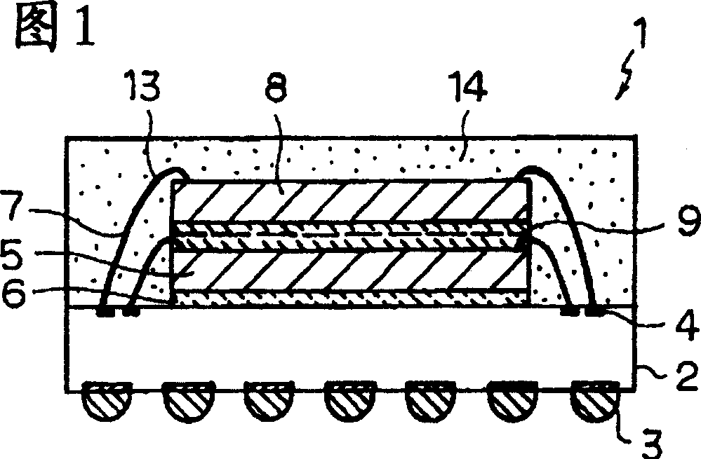
[0053] Hereinafter, modes for implementing the present invention will be described with reference to the drawings. In addition, although embodiment of this invention is described based on drawings below, these drawings are provided for illustration, and this invention is not limited to these drawings.

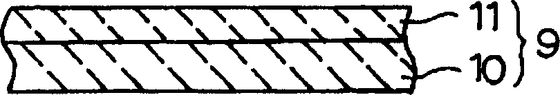
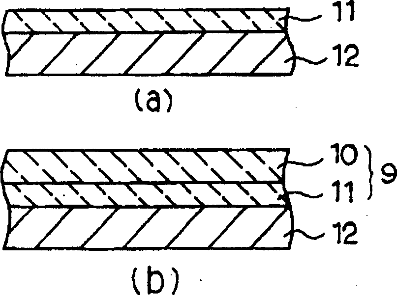
[0054] FIG. 1 is a cross-sectional view showing a schematic configuration of a semiconductor device according to a first embodiment of the present invention. A semiconductor device (semiconductor package) 1 shown in the figure has a circuit board 2 as an element mounting substrate. As the circuit board 2 , a substrate made of various materials such as a resin substrate, a ceramic substrate, and a glass substrate can be used. As the resin substrate, a common multilayer copper-clad laminate (multilayer printed wiring board) or the like is used. On the lower surface side of the circuit board 2, external connection terminals 3 such as solder bumps are formed. In addition, on the...


PUM


Abstract

The invention provides a semiconductor device, which is characterized by including a substrate with an electrode section; a first semiconductor component, which has a first electrode solder pad connected on the electrode section by a first bonding lead, and is adhered onto the substrate; and a second semiconductor component, which has a second electrode solder pad connected on the electrode section by a second bonding lead, and is adhered onto the first semiconductor component by an adhesive agent layer which has a two-layer structured formed by the same material and having different elastic rates.

Description

technical field [0001] The present invention relates to a semiconductor device in which a plurality of semiconductor elements are stacked. Background technique [0002] In recent years, a stacked multi-chip package in which a plurality of semiconductor elements (semiconductor chips) are stacked and packaged in a single package has been put into practical use in order to achieve miniaturization and high-density packaging of semiconductor devices. In such a stacked multi-chip package, a plurality of semiconductor elements are sequentially stacked on a mounting substrate such as a circuit board through an adhesive such as a die-bonding material, and the electrodes of each semiconductor element are electrically connected by bonding wires. Electrode parts such as pads and circuit boards. In addition, by encapsulating such a laminated structure with a sealing resin, a laminated multi-chip package is constituted. [0003] However, in the stacked multi-chip package described above...

Claims


Application Information

Patent Timeline
IPC IPC(8): H01L25/065
CPCH01L2224/73265H01L2224/32145H01L2224/48227H01L2224/32225H01L2225/06562H01L2224/92247H01L24/73H01L2924/00012H01L2924/00
Inventor 芳村淳小牟田直幸沼田英夫
Owner KK TOSHIBA
Features
  • Generate Ideas
  • Intellectual Property
  • Life Sciences
  • Materials
  • Tech Scout
  • Unparalleled Data Quality
  • Higher Quality Content
  • 60% Fewer Hallucinations
Learn More