Chip integrated waveguide multiplexer
A substrate-integrated waveguide and integrated waveguide technology, which is applied to waveguide devices, waveguides, electrical components, etc., can solve the problems of difficult processing of multiplexers, large external radiation, and large insertion loss, and achieve easy integration and high Q value , low loss effect
- Summary
- Abstract
- Description
- Claims
- Application Information
AI Technical Summary
Problems solved by technology
Method used
Image
Examples
Embodiment 1
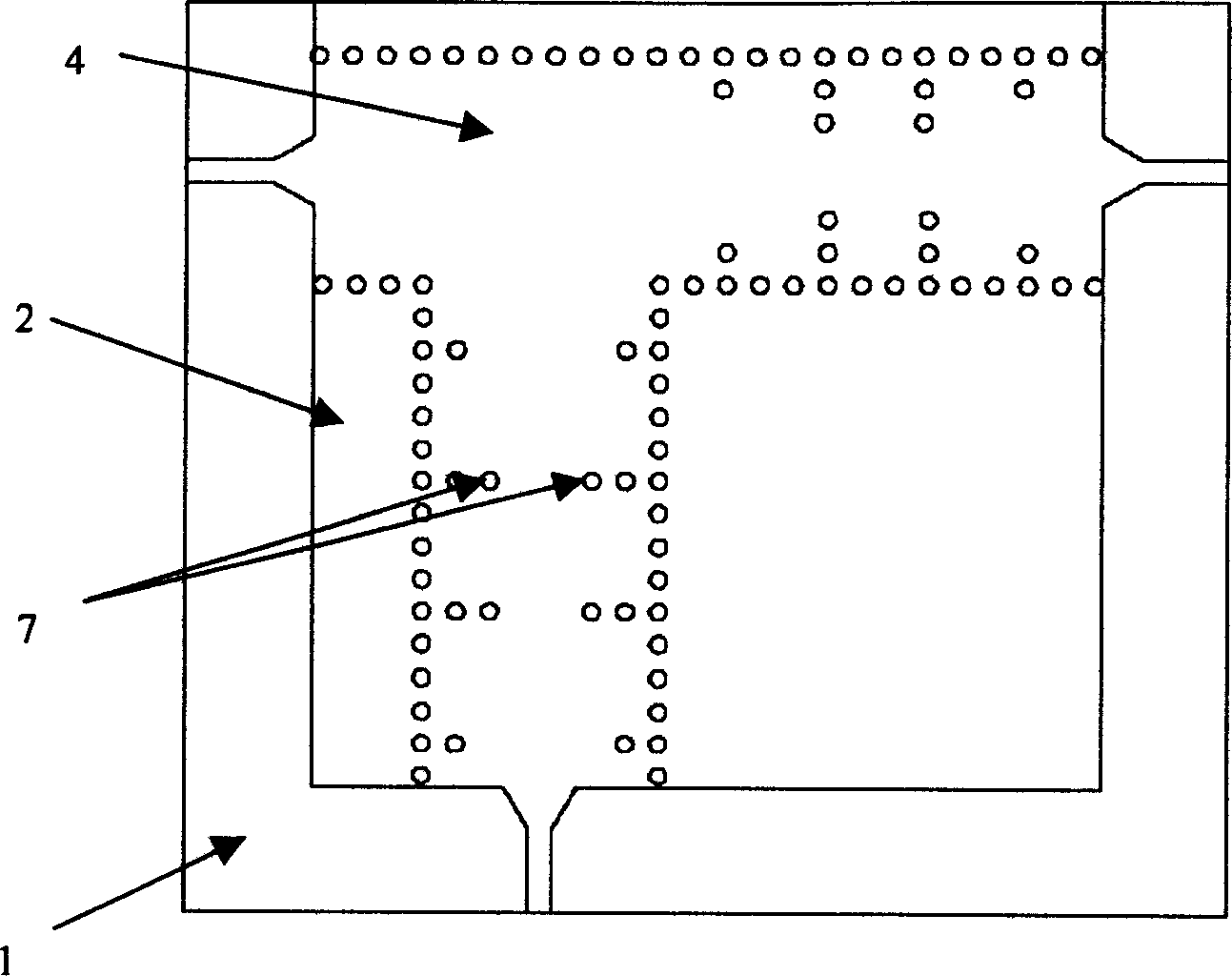
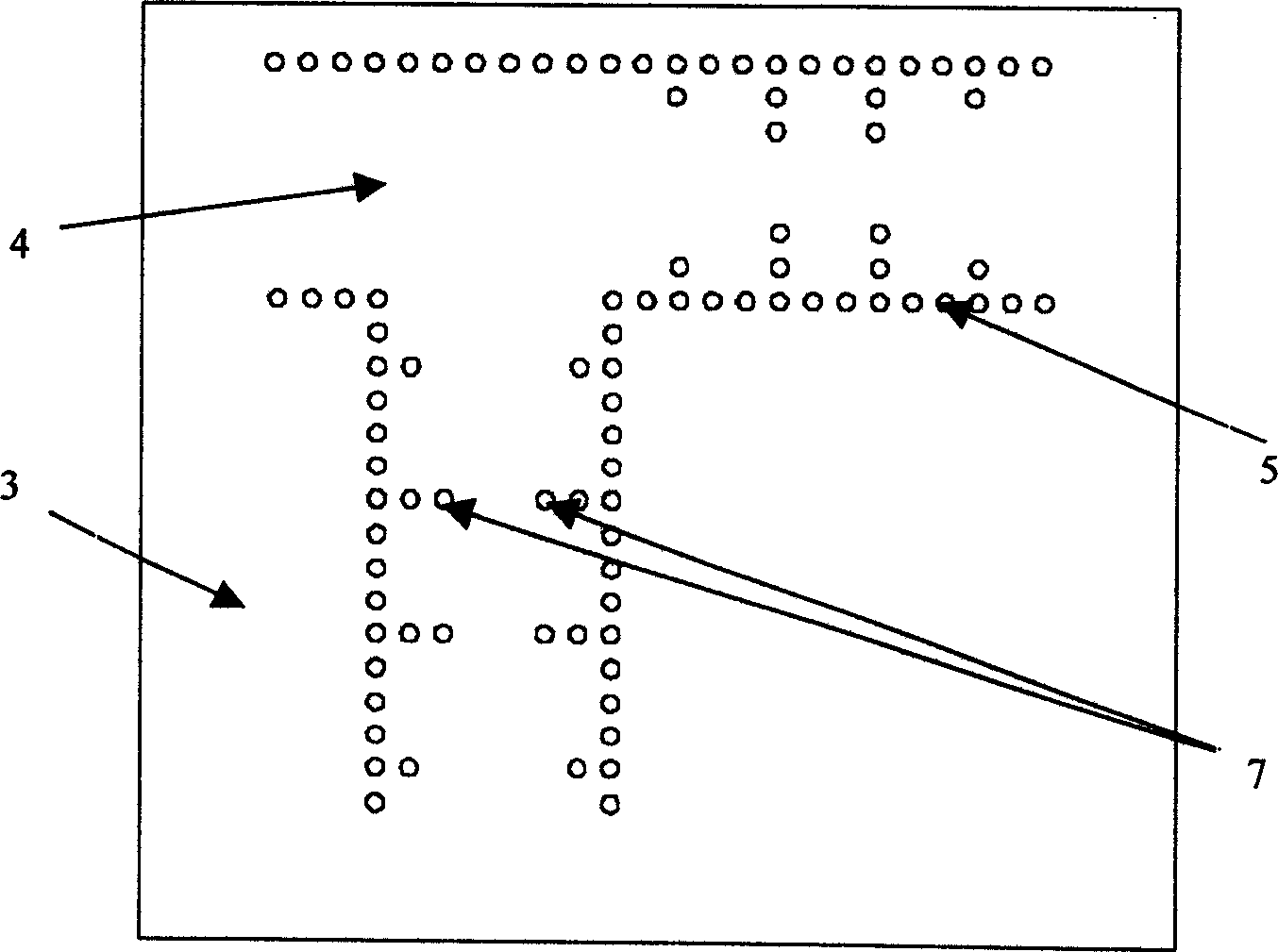
[0019] A substrate integrated waveguide multiplexer for feeding a microstrip antenna, comprising a dielectric substrate 1 covered with metal patches 2 and 3 on both sides, a main waveguide 4 is provided on the dielectric substrate 1, and a main waveguide 4 At least one sub-waveguide is connected to the sub-waveguide and one end of each sub-waveguide is connected to the main waveguide 4, the other end of each sub-waveguide is respectively connected with a substrate integrated waveguide cavity, and one end of the substrate integrated waveguide cavity is provided with The inductive window 7 for coupling of the sub-waveguides, the main waveguide 4 and the sub-waveguides are all composed of two rows of metallized through holes arranged on the dielectric substrate 1. One end of the main waveguide 4 is the input end, and the other end of the substrate integrated waveguide cavity As the output end, the substrate integrated waveguide cavity is enclosed by metallized through holes provided ...
Embodiment 2
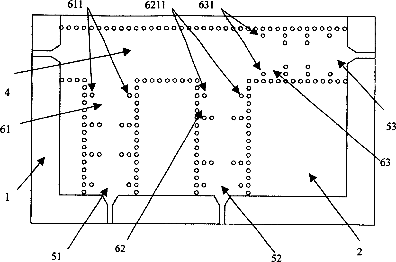
[0021] The multiplexer of the present invention includes a duplexer, a triplexer, a quadruple or a (N-1) multiplexer (N is the number of ports). The following is a detailed description of the triplexer (see figure 1 ):
[0022] A substrate-integrated waveguide 3 multiplier for feeding a microstrip antenna, comprising a dielectric substrate 1 covered with metal patches 2 and 3 on both sides, a main waveguide 4 is provided on the dielectric substrate 1, and a main waveguide 4 Three sub-waveguides 51, 52, 53 are connected to the upper side, and one end of the three sub-waveguides 51, 52, 53 is connected to the main waveguide 4, and the other ends of the three sub-waveguides are respectively connected to the substrate integrated waveguide cavity 61 , 62, 63, one end of the substrate integrated waveguide cavity 61, 62, 63 is provided with inductive windows 611, 621, 631 for coupling with the sub-waveguides, the main waveguide 4 and the sub-waveguides are both set on the dielectric sub...
PUM
| Property | Measurement | Unit |
|---|---|---|
| Reflection coefficient | aaaaa | aaaaa |
Abstract
Description
Claims
Application Information
 - R&D
- Intellectual Property
- Life Sciences
- Materials
- Tech Scout
- Unparalleled Data Quality
- Higher Quality Content
- 60% Fewer Hallucinations
Browse by: Latest US Patents, China's latest patents, Technical Efficacy Thesaurus, Application Domain, Technology Topic, Popular Technical Reports.
© 2025 PatSnap. All rights reserved.Legal|Privacy policy|Modern Slavery Act Transparency Statement|Sitemap|About US| Contact US: help@patsnap.com


