Semiconductor wafer and production method thereof

A technology of semiconductors and wafers, applied in the field of semiconductor wafers and their manufacturing, can solve the problem of wasting limited space on chips

Inactive Publication Date: 2005-12-07
ADVANCED ANALOG TECH INC
View PDF0 Cites 0 Cited by
  • Summary
  • Abstract
  • Description
  • Claims
  • Application Information

AI Technical Summary

Problems solved by technology

Therefore, the terminal pads waste the limited space of each of the chips

Method used


Image

  • Semiconductor wafer and production method thereof
  • Semiconductor wafer and production method thereof
  • Semiconductor wafer and production method thereof

Examples


Embodiment Construction

[0026] This case can be obtained through the following icons and detailed descriptions:

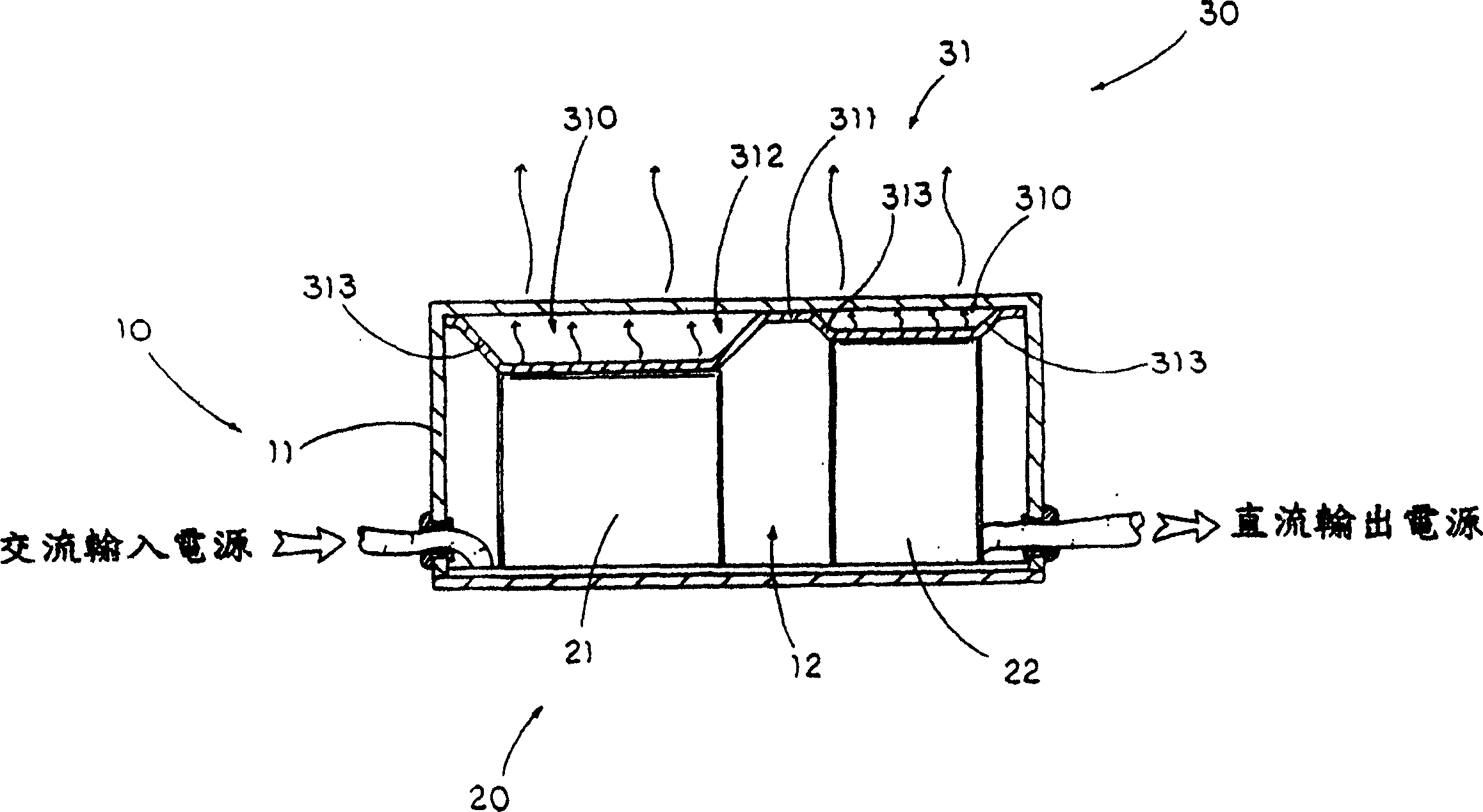
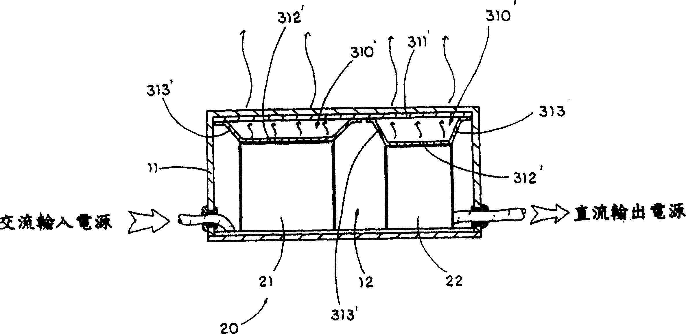
[0027] refer to figure 1 , is the top view of the semiconductor wafer of the preferred embodiment of the present case. Wherein, the semiconductor wafer includes a wafer body 10 and a plurality of analog IC chips 20 spaced and aligned on the wafer body 10 , and a region between every two chips 20 is defined as a dicing line 11 . Wherein, each of the chips 20 has an internal circuit 21 formed inside the chip and at least one terminal pad 22 formed along the dicing line 11 .

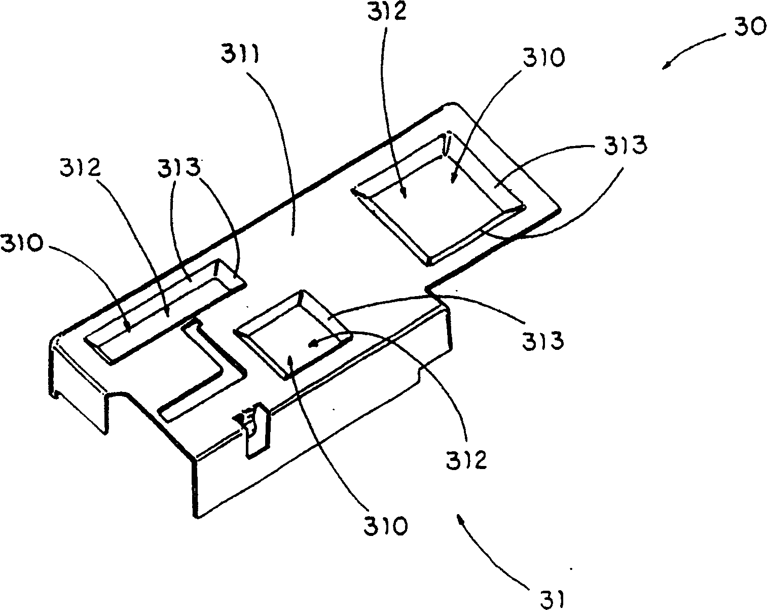
[0028] The semiconductor wafer further includes a conductive arrangement 30 comprising at least one conductive component 31 formed on the wafer body 10 to electrically connect the terminal pads 22 to the internal circuit 21 so that when the chip 20 is separated from the After cutting off the wafer body 10 , the terminal pads 22 can be cut off from the chip 20 so that the internal circuit 21 remains in the chip 20 . ...


PUM


Abstract

A semiconductor wafer and making method thereof, which contains a wafer main unit, plurality of analog IC chip on chip with cutting channel between every two chips, each chip has internal circuit, at least one terminal pad and a conductor consisting of conductive assembly, keeping terminal pad conduction with internal circuit of chip, removing terminal pad from chip after cutting off chip from wafer along the channel and keeping internal circuit in chip. The making method contains 1, forming plurality of analog chips on wafer in equal interval, defining all cutting channel between every two chips, forming internal circuit terminal pad, 2, arranging said terminal pad along cutting channel near the wafer unit, 3, forming conductive assembly on wafer, 4, cutting off chip from wafer unit.

Description

technical field [0001] The present invention is related to semiconductors, in particular to a semiconductor wafer and a manufacturing method thereof. Background technique [0002] A conventional semiconductor wafer includes a wafer body and a plurality of chips formed at intervals on the wafer body for defining a dicing line as a boundary between every two chips. Therefore, each of these chips (also referred to as an analog IC chip) is an integrated circuit based on a silicon substrate. [0003] Before each of the chips is diced into an individual component, a wafer test must be performed to ensure that each of the chips is functioning under an optimal condition. Generally speaking, each of these chips includes a plurality of bonding pads (bond pads) and a plurality of terminal pads formed at intervals inside the chip, wherein the terminal pads can be test pads (test pads) for A pin card or a trim pad is used to measure the voltage of the chip to adjust the reference volta...

Claims


Application Information

Patent Timeline
Patent Type & Authority Applications(China)
IPC IPC(8): H01L27/00
Inventor 陈维忠张咏青黄照兴方振宇余建朋
Owner ADVANCED ANALOG TECH INC
Why Eureka
Try Eureka