Standard cell, semiconductor integrated circuit device of standard cell scheme and layout design method for semiconductor integrated circuit device

一种标准单元、电势的技术,应用在半导体器件、半导体/固态器件制造、电固体器件等方向,能够解决动态节点反相、电路故障、电路工作容限降低等问题

Inactive Publication Date: 2005-12-14
SOCIONEXT INC
View PDF1 Cites 2 Cited by
  • Summary
  • Abstract
  • Description
  • Claims
  • Application Information

AI Technical Summary

Problems solved by technology

[0007] With a dynamic circuit to which such precharging is applied, a higher circuit operating speed can be obtained, but the following problem arises: when there is capacitive coupling between a dynamic node inside the circuit and its adjacent wirings, During the period, the potential of the dynamic node changes under the influence of the potential change of the connecting lines, thereby causing the reduction of the circuit operating margin, and causing the circuit failure
In this case, a side coupling capacitance appears between the adjacent wiring between the dynamic node and the standard cell, and the potential change of the wiring between the standard cells is transmitted to the dynamic node through the side coupling capacitance, and the potential of the dynamic node may Can reverse phase (i.e., may cause circuit malfunction)

Method used


Image

  • Standard cell, semiconductor integrated circuit device of standard cell scheme and layout design method for semiconductor integrated circuit device
  • Standard cell, semiconductor integrated circuit device of standard cell scheme and layout design method for semiconductor integrated circuit device
  • Standard cell, semiconductor integrated circuit device of standard cell scheme and layout design method for semiconductor integrated circuit device

Examples


no. 1 example

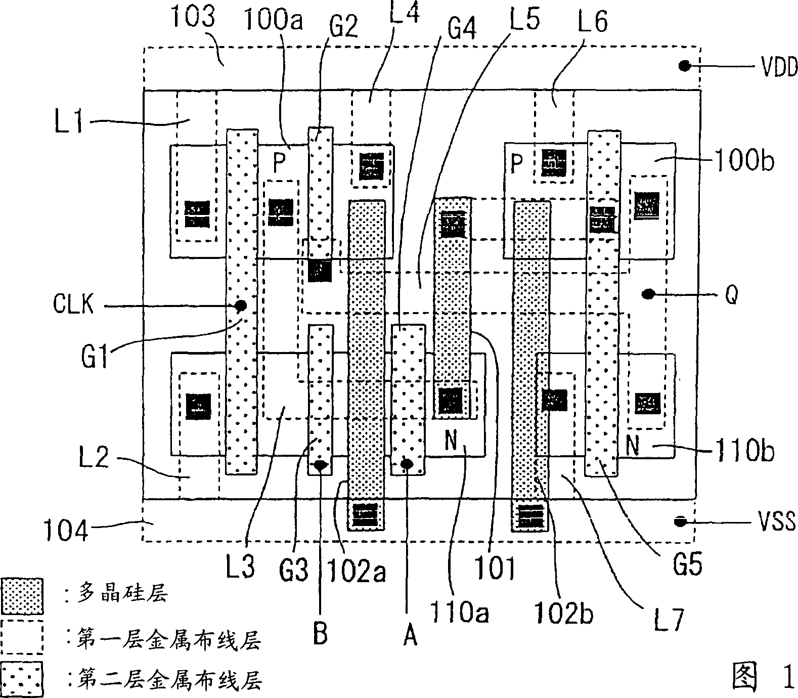
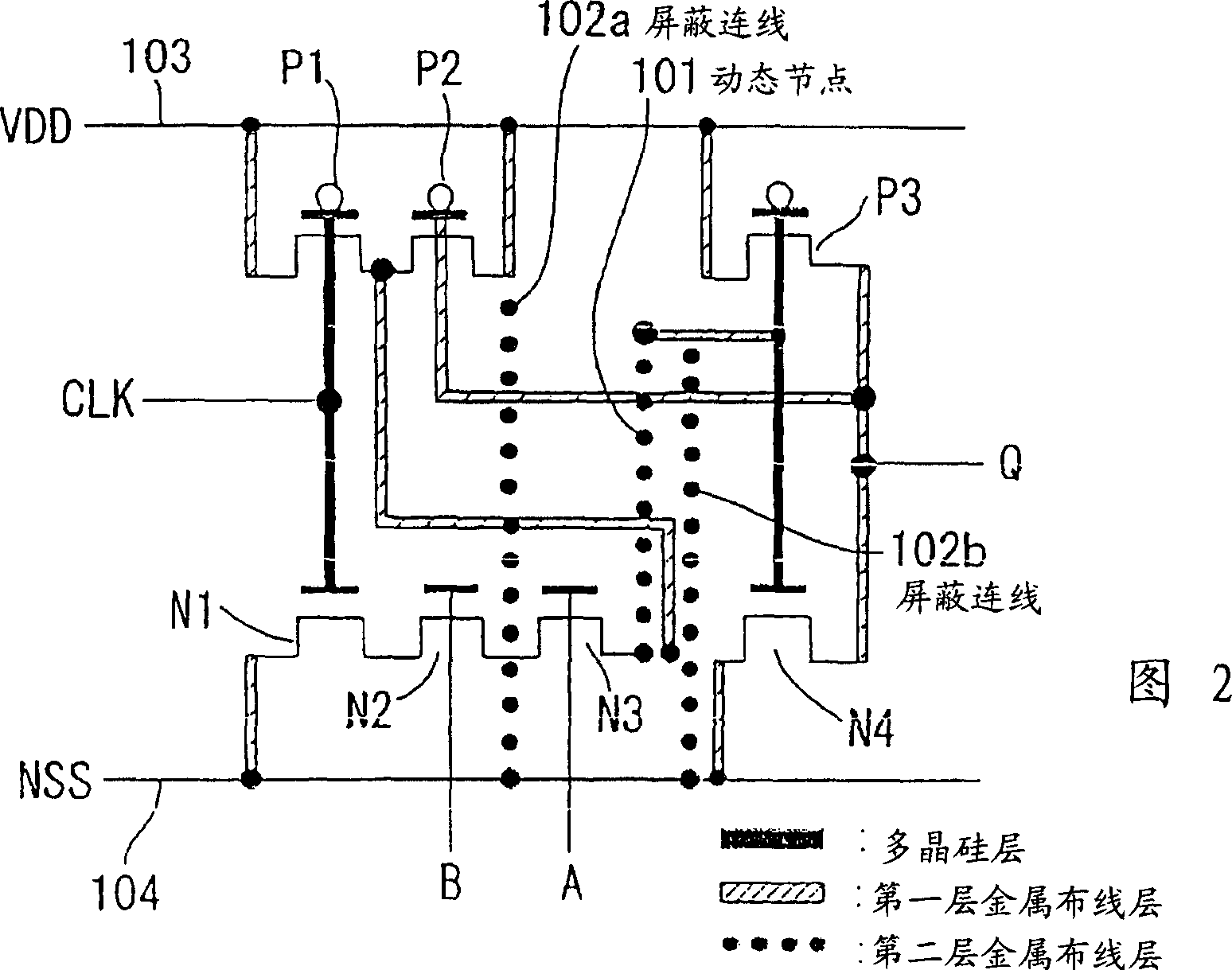
[0032] 1 is a layout showing an example of the layout of diffusion regions, metal wiring layers, etc. of a standard cell of the present invention in which a dynamic 2-input AND circuit is constructed. FIG. 2 is a circuit diagram showing the transistors constituting the dynamic 2-input AND circuit shown in the layout of FIG. 1 and the interconnections interconnecting the transistors at the same stage. FIG. 1 and FIG. 2 are equivalent, and FIG. 2 is prepared to facilitate understanding of the content of the layout of FIG. 1 .

[0033] The circuits shown in Figures 1 and 2 correspond to the previously described Figure 5 The dynamic 2-input AND circuit shown is the same. However, in FIGS. 1 and 2, shield wirings (102a, 102b) fixed to the ground potential are respectively formed on the left and right sides of the dynamic node (101) to prevent the potential of the dynamic node (101) from becoming unstable. (This will be explained below).

[0034] Conditions of the wiring layout i...

no. 2 example

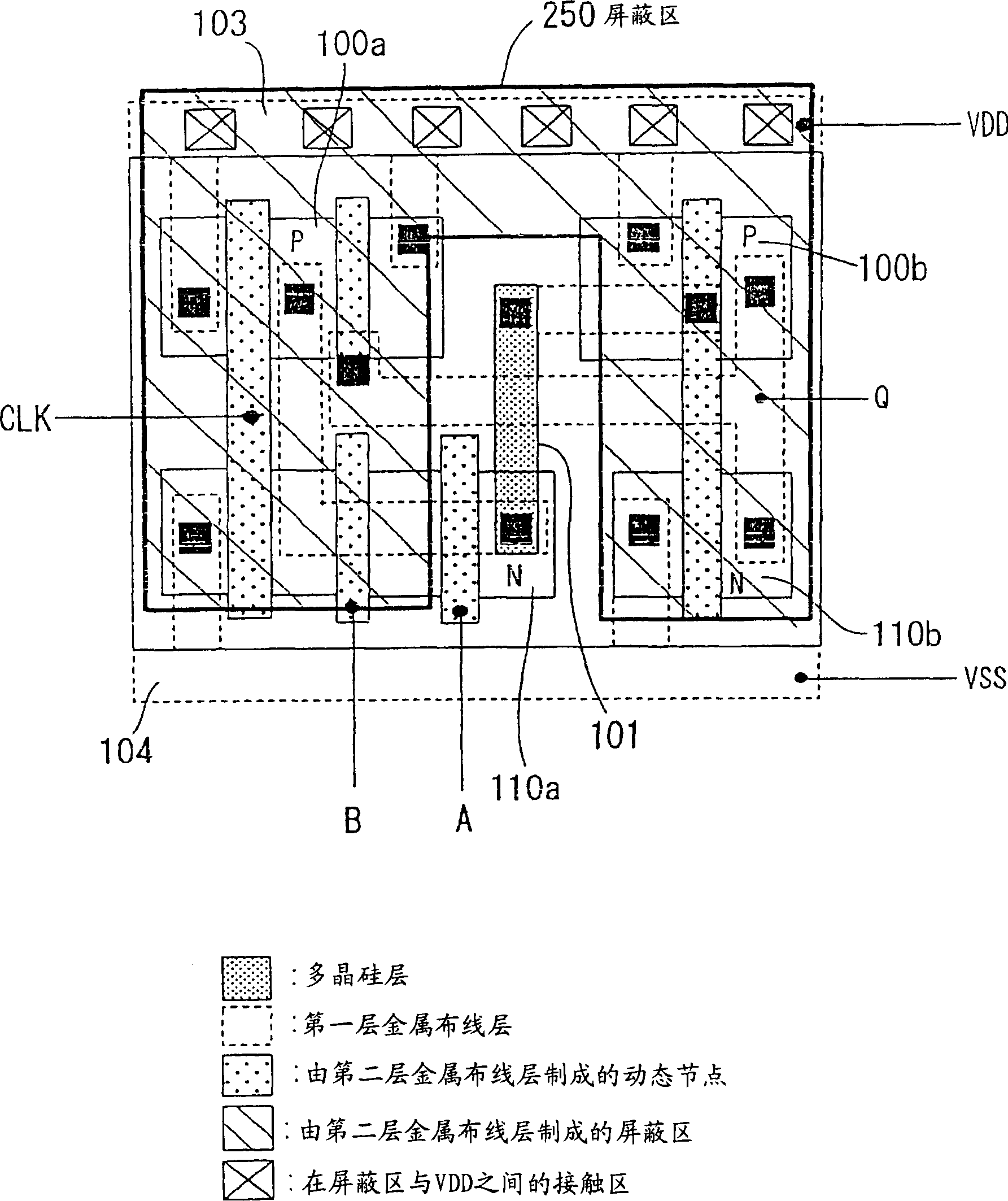
[0046] image 3 is a layout showing another example of the layout of diffusion regions, metal wiring layers, etc. of a standard cell of the present invention in which a dynamic 2-input AND circuit is constructed. In this embodiment, the "shield connection" is replaced with a larger area "shield area". exist image 3 In , the same reference numerals and numerals are assigned to the same parts as in the previous figures, and the layout situation is also the same as in the previous embodiments.

[0047] exist image 3 In , the shielding region 250 made of the second metal wiring layer at the same level as the dynamic node 101 is provided. The shielding region 250 is disposed substantially over the entire area of ​​the standard cell so as to surround the dynamic node 101 . The shielding area 250 is connected to the VDD line (103) through a plurality of contact areas. As the shielding region 250, the same material as that of the metal wiring (for example, aluminum) spreads ove...

no. 3 example

[0050] Figure 4 is a layout showing another example of the layout of diffusion regions, metal wiring layers, etc. of a standard cell of the present invention in which a dynamic 2-input AND circuit is constructed. In this embodiment, a "wiring keepout area" is used instead of a shield wiring or a shield area, whereby the same advantages as in each of the foregoing embodiments are obtained.

[0051] exist Figure 4 , the dynamic node 101 is surrounded by a region (wiring forbidden region) 300 having a predetermined area made of a wiring layer (second metal wiring layer) at the same level as the any wiring used to interconnect standard cells). Therefore, in automatic place and route, the wires (second-level routing layer) used to interconnect standard cells do not pass through the area adjacent to the dynamic node 101 (area so close that the dynamic node due to side coupling coupling to another wire can cause problems).

[0052] exist Figure 4In , the connection line 106 b...


PUM


Abstract

The invention prevents the potential inversion of the dynamic nodes due to the fact that any connection between standard cells made on the same level as the wiring layer of the dynamic nodes inside the standard cells is arranged to be the same as Dynamic nodes are adjacent. Near the dynamic node 101 inside the standard cell, shielded wirings 102a and 102b made of wiring layers at the same level as the dynamic node are provided, thereby preventing any wiring between standard cells from passing adjacent to the dynamic node. The shielded wiring can be replaced by a shielded area or a wiring keepout area.

Description

technical field [0001] The invention relates to a standard cell, a semiconductor integrated circuit device of the standard cell scheme, and a layout design method for the semiconductor integrated circuit device. Background technique [0002] The standard cell scheme is one of techniques used to design large scale integration (LSI). In the standard cell scheme, a desired circuit is constructed by preparing in advance various small-scale circuits called "standard cells" and then combining them. In the layout design of an LSI for a standard cell scheme, automatic placement and wiring to which a software tool is applied is performed. In the layout design of the automatic placement and routing scheme, various circuits of different functions are constructed in a short time by arranging standard cells on a semiconductor substrate and performing wiring between standard cells according to specifications. [0003] In an LSI based on automatic placement and routing of the prior art, ...

Claims


Application Information

Patent Timeline
Patent Type & Authority Applications(China)
IPC IPC(8): H01L21/822G11C5/06G11C11/24H01L21/82H01L27/02H01L27/04H01L27/118H03K19/00H03K19/096
CPCG11C5/063H01L27/0207H01L27/11807
Inventor 农添三资木村纪之中田充香
Owner SOCIONEXT INC
Why Eureka
Try Eureka