Method for producing a semiconductor element

A technology for semiconductors and devices, applied in the field of manufacturing semiconductor devices, can solve the problems of limited thermal conductivity and electrical conductivity of adhesives, heat resistance, limited reliable temperature range, power loss, etc.

Inactive Publication Date: 2010-06-23
OSRAM OPTO SEMICONDUCTORS GMBH
View PDF8 Cites 0 Cited by
  • Summary
  • Abstract
  • Description
  • Claims
  • Application Information

AI Technical Summary

Problems solved by technology

At higher electrical powers, problems may arise due to the limited thermal and electrical conductivity of the adhesive
Furthermore, the limited heat resistance of such adhesive connections also limits the reliable temperature range of the corresponding device and thus limits the maximum possible power loss

Method used


Image

  • Method for producing a semiconductor element
  • Method for producing a semiconductor element
  • Method for producing a semiconductor element

Examples


Embodiment Construction

[0083] In the figures, identical elements or identically acting elements are marked with the same reference signs.

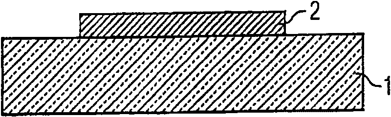
[0084] In the first step of the method shown in the figure, Figure 1A , a semiconductor layer 2 is provided on a substrate 1 . The semiconductor layer 2 may be a nitride compound semiconductor layer, such as an InGaN layer epitaxially grown on a sapphire substrate. Furthermore, the semiconductor layer 2 can also comprise a plurality of individual layers which can contain, for example, GaN, AlN, AlGaN, InGaN, InN or InAlNGaN and which are grown successively on the substrate 1 .

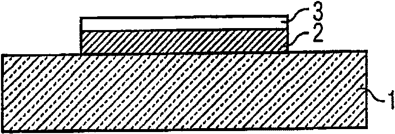
[0085] In the next step, Figure 1B , the semiconductor layer 2 is provided with a contact metallization layer 3 on the side facing away from the substrate. A very low contact resistance is achieved by means of the contact metallization layer 3 between the semiconductor layer 2 and an electrical connection, for example a connecting line, which is provided in a later method step. Fur...


PUM


Abstract

A method for producing a semiconductor component, in particular a thin-film component, a semiconductor layer being separated from a substrate by irradiation with a laser beam having a plateaulike spatial beam profile. Furthermore, the semiconductor layer, prior to separation, is applied to a carrier with an adapted thermal expansion coefficient. The method is suitable in particular for semiconductor layers containing a nitride compound semiconductor.

Description

technical field [0001] The present invention relates to a method of manufacturing a semiconductor device in which a semiconductor layer is separated from a substrate by irradiation with a laser beam. Background technique [0002] Such methods are used, for example, for the production of substrate-free light-emitting diodes on the basis of GaN. Such a component comprises a semiconductor body part and a carrier part, on which the semiconductor body is fastened. To produce the semiconductor body, first the semiconductor layers are produced on a suitable substrate, then connected to the carrier, and then separated from the substrate. By slicing, for example by sawing, the carrier with the semiconductor layer arranged thereon, a plurality of semiconductor bodies are produced, each fastened on the respective carrier. It is important here that the substrate used for the production of the semiconductor layer is separated from the semiconductor layer without at the same time servin...

Claims


Application Information

Patent Timeline
IPC IPC(8): H01L31/18H01L33/00H01L21/78B23K26/00H01L21/762H01L21/20C30B33/00
CPCB23K26/073B23K26/0738B23K26/0732C30B29/42C30B29/403H01L33/0079C30B29/406H01L21/76251H01L21/2007C30B33/00H01L24/83H01L33/0093
Inventor M·费雷尔B·哈恩V·海勒S·凯泽F·奥特A·普勒斯尔
Owner OSRAM OPTO SEMICONDUCTORS GMBH
Why Eureka
Try Eureka