Transferring method of thin film device, production method of active matrix substrate

An active matrix and transfer method technology, which is applied in semiconductor/solid-state device manufacturing, optics, instruments, etc., can solve problems such as difficulties and achieve the effect of preventing the deterioration of characteristics

Inactive Publication Date: 2006-02-15
SAMSUNG ELECTRONICS CO LTD
View PDF2 Cites 10 Cited by
  • Summary
  • Abstract
  • Description
  • Claims
  • Application Information

AI Technical Summary

Problems solved by technology

This point becomes a big disadvantage when mounting a substrate on which a thin film device such as a TFT is formed on an electronic device.
That is, there is a gap between the constraints caused by manufacturing conditions and the more ideal characteristics required for products, and it is extremely difficult to satisfy both of these conditions or characteristics

Method used


Image

  • Transferring method of thin film device, production method of active matrix substrate
  • Transferring method of thin film device, production method of active matrix substrate
  • Transferring method of thin film device, production method of active matrix substrate

Examples


Embodiment 1

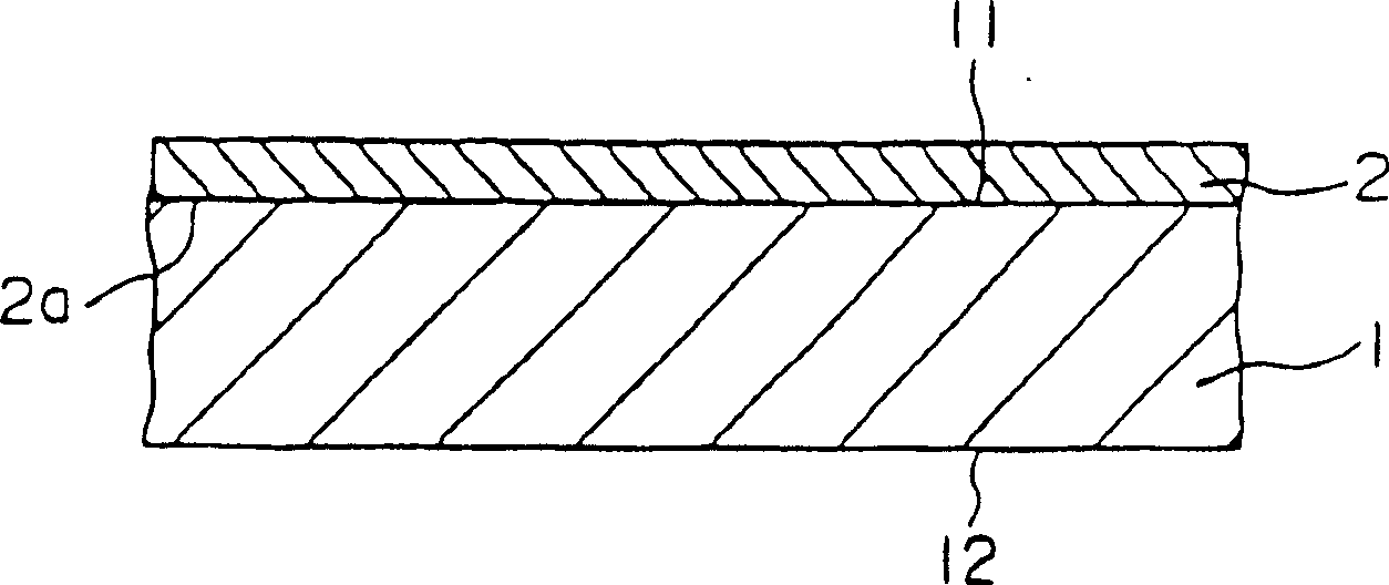
[0162] A quartz substrate (softening point: 1630° C., deformation point: 1070° C., excimer laser transmittance: approximately 100%) of 50 mm in length × 50 mm in width × 1.1 mm in thickness was prepared, and on one surface of the quartz substrate, the Low pressure CVD method (Si 2 h 6 gas, 425°C) to form an amorphous silicon (a-Si) film as a separation layer (laser absorbing layer). The film thickness of the separation layer was 100 nm.

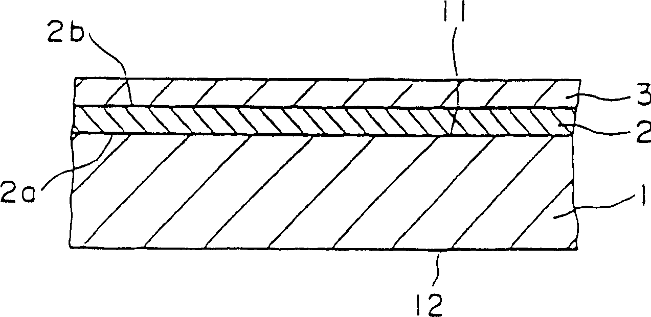
[0163] Secondly, on the separation layer, the ECR-CVD method (SiH 4 +O 2 gas, 100°C) to form SiO 2 membrane as an intermediate layer. The film thickness of the intermediate layer was 200 nm.

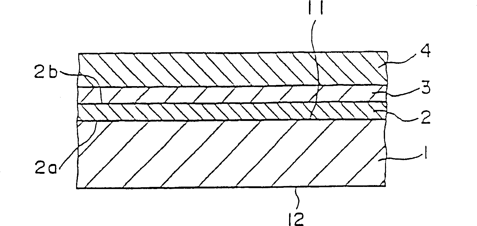
[0164] Secondly, use CVD method on the intermediate layer (Si 2 h 6 gas) to form a polysilicon film with a film thickness of 50 nm as the transferred layer. Thereafter, a predetermined pattern is etched on the polysilicon film to form regions to be source, drain, and channel of the thin film transistor. Thereafter, the surface of the polysilic...

Embodiment 2

[0173] Transfer of the thin film transistor was performed in the same manner as in Example 1 except that the separation layer was made of an amorphous silicon film containing 20 at % H (hydrogen). In addition, the amount of H in the amorphous silicon film is adjusted by appropriately setting the conditions at the time of film formation by the low-pressure CVD method.

Embodiment 3

[0175] In addition to making the separation layer a ceramic thin film (composition: PbTiO 3 , film thickness: 200 nm), the transfer of the thin film transistor was carried out in the same manner as in Example 1.


PUM

PropertyMeasurementUnit
softening pointaaaaaaaaaa
wavelengthaaaaaaaaaa

Abstract

A transfer method comprising: providing a substrate; forming a transferred layer on the substrate; combining a transfer body with the transferred layer; and removing the transferred layer from the substrate, and transferring the transferred layer to the Transfer body; re-use the above substrate for another transfer.

Description

[0001] This application is a divisional application of the parent application with the application number 03157964.7 and the application date of August 30, 2003. The first prior application of the parent application is JP96-225643, and the earlier application date is August 27, 1996 . technical field [0002] The present invention relates to a peeling method of a peeled object, and in particular to a transfer method of peeling a transferred layer made of a thin film such as a functional film and transferring it to a transfer body such as a transparent substrate. In addition, the present invention relates to a transfer method of a thin film device and a thin film device, a thin film integrated circuit device, and a liquid crystal display device manufactured by the method. Background technique [0003] For example, when a liquid crystal display using a thin film transistor (TFT) is manufactured, a process of forming a thin film transistor on a transparent substrate by a CVD me...

Claims


Application Information

Patent Timeline
Patent Type & Authority Applications(China)
IPC IPC(8): H01L21/84H01L21/762G02F1/1362G02F1/1368
Inventor 下田达也井上聪宫泽和加雄
Owner SAMSUNG ELECTRONICS CO LTD
Why Eureka
Try Eureka