Charge pump circuit

A charging pump and circuit technology, applied in logic circuits, electrical components, static memory, etc., can solve problems such as insufficient regulators

Inactive Publication Date: 2006-02-15
SANYO ELECTRIC CO LTD
View PDF1 Cites 4 Cited by
  • Summary
  • Abstract
  • Description
  • Claims
  • Application Information

AI Technical Summary

Problems solved by technology

[0003] However, when the output voltage of the charge pump circuit does not want to be adjusted very high, when it is desired to ignore the capacitance value of the smoothing capacitor connected to the output of the charge pump circuit in the previous stage of the regulator, the output voltage is used as the transistor When the power supply voltage is supplied and the transistor is to be operated optimally, the conventional regulator is not sufficient, and it is necessary to improve stability by feedback control

Method used


Image

  • Charge pump circuit
  • Charge pump circuit

Examples


Embodiment Construction

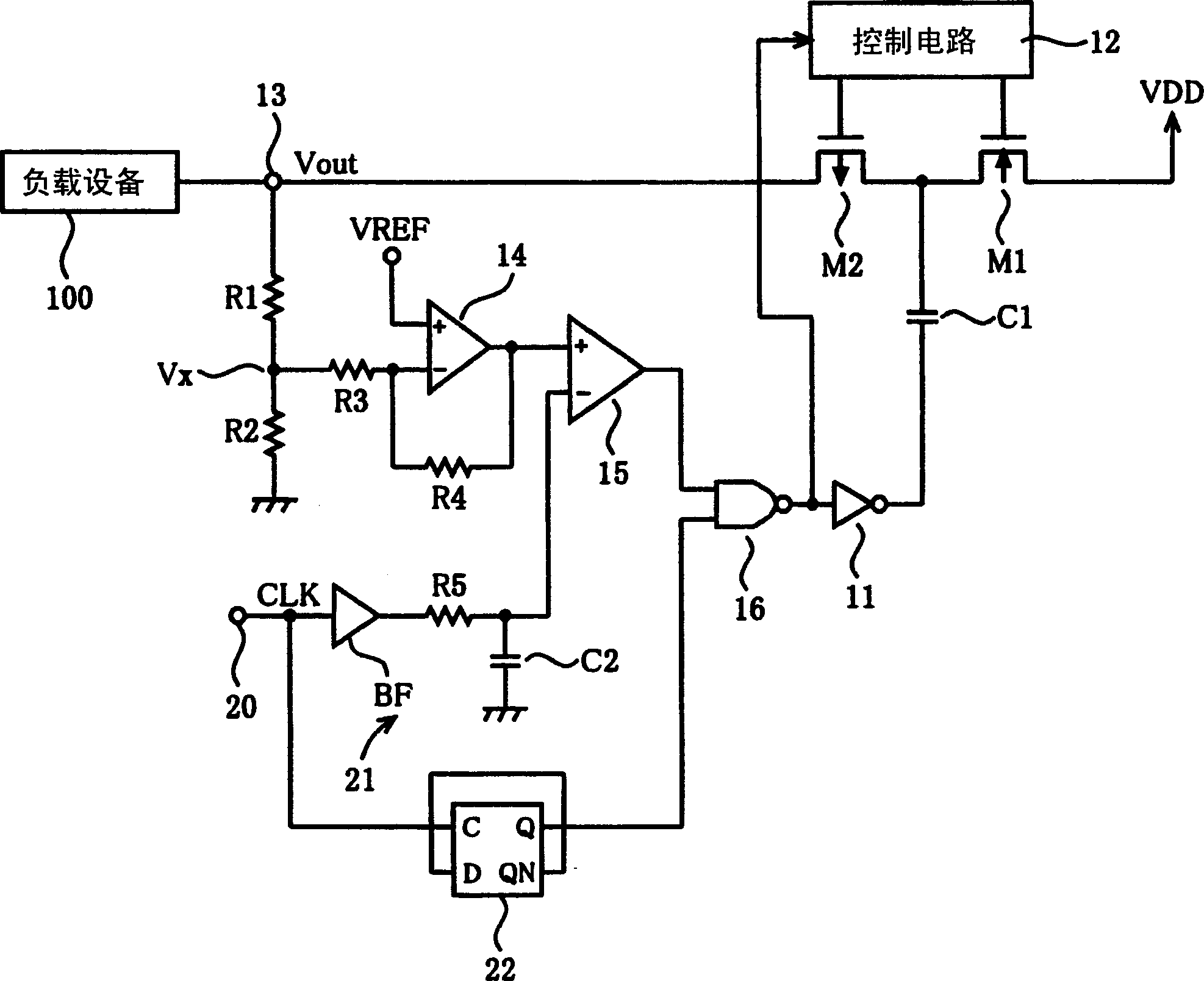
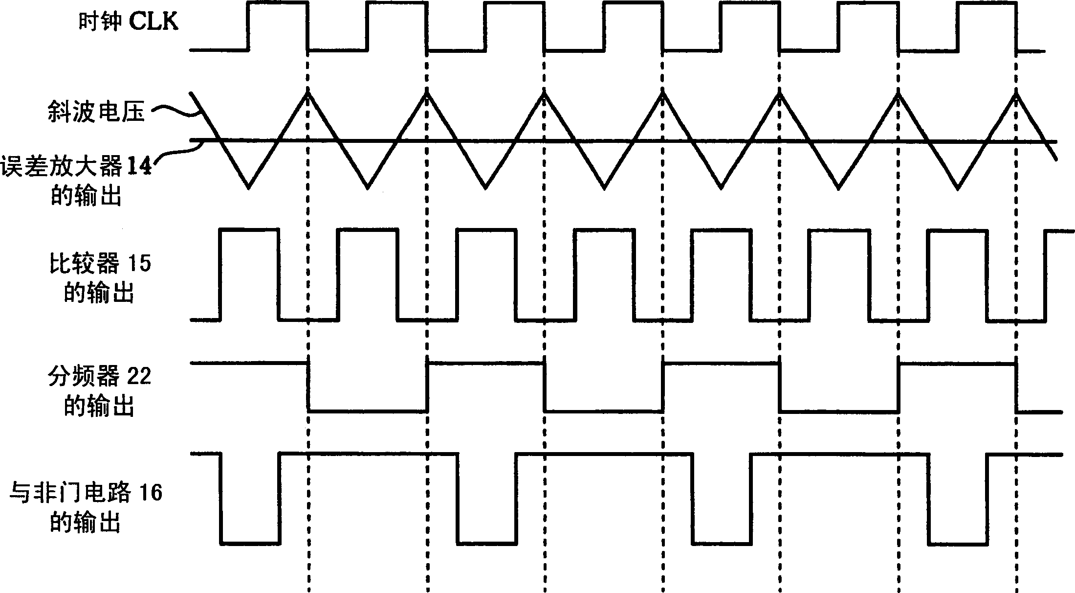
[0011] Hereinafter, embodiments of the present invention will be described with reference to the drawings. The first charge transfer MOS transistor M1 and the second charge transfer MOS transistor M2 are connected in series, and the power supply voltage VDD as an input voltage is supplied to the source of the first charge transfer MOS transistor M1.

[0012] Here, the first charge transfer MOS transistor M1 may be of the N-channel type or the P-channel type, and the second charge transfer MOS transistor M2 is preferably of the P-channel type. This is because, if the second charge transfer MOS transistor M2 is an N-channel type, a high voltage for turning it on cannot be obtained from this circuit.

[0013] A connection point between the first charge transfer MOS transistor M1 and the second charge transfer MOS transistor M2 is connected to the first terminal of the capacitor C1. The clock from the clock driver 11 is applied to the second terminal of the capacitor C1 . The cl...


PUM


Abstract

The charge pump circuit comprises first and second charge transferring MOS transistors M1, M2 connected in series; a capacitor C1 connected at its first terminal to the connection point of the MOS transistors M1, M2; an integrating circuit 21 that generates a ramp voltage corresponding to a clock CLK; a comparator 15 that compares the ramp voltage with a voltage corresponding to an output voltage Vout from the second MOS transistor M2; a frequency divider 22 that divides the clock CLK into a half; and a NAND circuit 16 that masks an output of the comparator 15 according to a frequency-divided output of the frequency divider 22. The output of the NAND circuit 16 is impressed to the second terminal of the capacitor C1.

Description

technical field [0001] The invention relates to a charging pump circuit, in particular to a charging pump circuit whose output voltage has the function of regulating. Background technique [0002] A charge pump circuit consists of a charge transfer device, a capacitor, a clock driver, etc. It is a circuit that boosts an input voltage and outputs it, and is widely used in power supply circuits of transistor circuits, etc. Conventionally, in order to stabilize the output voltage of the charge pump circuit, an operational amplifier is used as a series regulator to adjust the output voltage to a desired constant voltage. A charge pump circuit using a regulator is described in Patent Document 1, for example. [0003] However, when the output voltage of the charge pump circuit does not want to be adjusted very high, when it is desired to ignore the capacitance value of the smoothing capacitor connected to the output of the charge pump circuit in the previous stage of the regulato...

Claims


Application Information

Patent Timeline
Patent Type & Authority Applications(China)
IPC IPC(8): H02M3/07
CPCG11C5/145H02M3/073H03K19/094H02M3/07
Inventor 河井周平
Owner SANYO ELECTRIC CO LTD
Why Eureka
Try Eureka