
Production of differential silica waveguide with high refractive index by ultraviolet laser written in

A high refractive index difference, silicon dioxide technology, applied in the direction of optical waveguide light guides, light guides, microlithography exposure equipment, etc., can solve the problem of not being able to prepare high refractive index difference waveguides, etc.

Inactive Publication Date: 2006-03-15
INST OF SEMICONDUCTORS - CHINESE ACAD OF SCI
View PDF0 Cites 3 Cited by
  • Summary
  • Abstract
  • Description
  • Claims
  • Application Information

AI Technical Summary

Problems solved by technology

But at present, the refractive index change that can be achieved by these two methods is 10 -4 ~10 -3 order of magnitude, which limits the method to fabricate waveguides with high refractive index difference

Method used


Image

  • Production of differential silica waveguide with high refractive index by ultraviolet laser written in
  • Production of differential silica waveguide with high refractive index by ultraviolet laser written in
  • Production of differential silica waveguide with high refractive index by ultraviolet laser written in

Examples


Embodiment 1

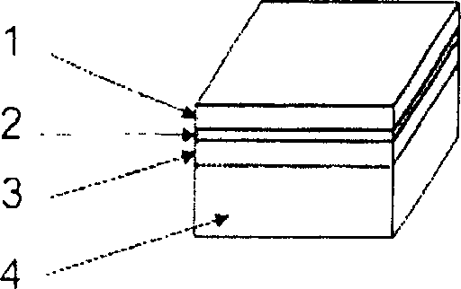
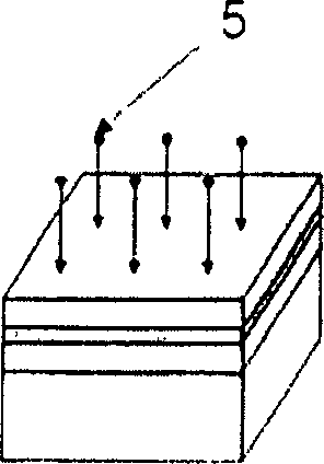
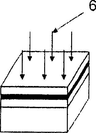
[0034] see figure 1 — Figure 5 .

[0035] First, the lower cladding layer 3, the waveguide layer 2 and the upper cladding layer 1 are sequentially grown on the silicon substrate by flame hydrolysis, and their thicknesses are respectively 15 μm, 6 μm, and 15 μm, wherein the waveguide layer 2 is doped with 8 mol.% germanium ( Ge) and an appropriate amount of B. Then put the substrate into a high-pressure container full of hydrogen 5, the pressure is 12MPa, and leave it at room temperature for two weeks. Uniformly expose the hydrogen-loaded substrate with ultraviolet laser 6, the exposure conditions are: wavelength 248nm, pulse frequency 20Hz, energy density 100mj / cm 2 / pulse, exposure time 30 minutes. A thin silicon wafer is used for deep etching, and the outer region 9 of the waveguide is hollowed out to form a mask 8, and the mask 8 is closely attached to the cladding on the substrate after the first exposure, and the entire substrate is exposed for the second time , for...

Embodiment 2

[0037] see figure 1 — Figure 5 .

[0038] First, the lower cladding layer 3, the waveguide layer 2 and the upper cladding layer 1 are sequentially grown on the silicon substrate by plasma-enhanced chemical vapor deposition, and their thicknesses are 15 μm, 6 μm, and 15 μm, respectively, and the waveguide layer is doped with 12 mol.% of Ge and a moderate amount of F. Then, the substrate was kept at 600° C. for 72 hours under a hydrogen atmosphere to carry hydrogen. Uniformly expose the hydrogen-loaded substrate with ultraviolet laser 6, the exposure conditions are: wavelength 244nm, pulse frequency 20Hz, energy density 100mj / cm 2 / pulse, exposure time 30 minutes. A layer of aluminum is plated on the substrate exposed for the first time, and then the film is subjected to photolithography and etching (etching away the film 9 in the non-waveguide region) to form a mask 8 . Then the whole substrate is exposed for the second time to form the waveguide 7 with high refractive in...

Embodiment 3

[0040] see figure 1 — Figure 5 . First, the lower cladding layer 3 and the waveguide layer 2 are sequentially grown on the silicon dioxide substrate by plasma enhanced chemical vapor deposition, and their thicknesses are respectively 15 μm and 8 μm, wherein the waveguide layer 2 is doped with 8 mol.% of Ge and an appropriate amount b. The upper cladding layer 1 of the waveguide is air. Then the substrate was uniformly scanned with a hydrogen flame 5 for 20 minutes to carry hydrogen. Use ultraviolet laser 6 to uniformly expose the hydrogen-loaded substrate, the exposure conditions are: wavelength 193nm, pulse frequency 20Hz, energy density 100mj / cm 2 / pulse, exposure time 30 minutes. A layer of polysilicon film is grown on the substrate exposed for the first time, and then the film is subjected to photolithography and etching (etching away the film 9 in the non-waveguide area) to form a mask 8 . Then the whole substrate is exposed for the second time to form the waveguid...


PUM

PropertyMeasurementUnit
wavelengthaaaaaaaaaa
thicknessaaaaaaaaaa

Abstract

A method for preparing silica wave guide with high refractivity difference by using ultraviolet layer write ¿C in includes forming substrate by growing silica bottom cladded, wave guide layer and top cladded in sequence on silicon or silica backing; loading hydrogen on said substrate; carrying out uniform exposure for substrate with ultraviolet laser to rise refractivity on wave guide layer uniformly; preparing mask and hollowing out its nonwaveguide region; covering wave guide region by mask and carrying out second time of exposure to lower refractivity at uncovered region; annealing for stabilizing refractivity variation.

Description

technical field [0001] The invention is used for making silicon dioxide optical waveguide devices, and particularly relates to the realization of high refractive index difference waveguides and waveguide devices by means of ultraviolet laser writing. Background technique [0002] At present, silica waveguides are usually prepared by etching. This process needs to go through a series of processes such as the growth of the lower cladding layer, the growth of the waveguide layer, the production of the mask plate, photolithography, development, etching, and the growth of the upper cladding layer. The process is not only complicated in process and high in production cost, but also requires very expensive equipment, which is not conducive to industrialized production. Since K.O. Hill discovered that ultraviolet laser exposure can change the refractive index of germanium-doped silicon dioxide material, a new method of making silicon dioxide waveguide——ultraviolet writing method has...

Claims


Application Information

Patent Timeline
Patent Type & Authority Applications(China)
IPC IPC(8): G02B6/02G02B6/00G03F7/20
Inventor 夏君磊吴远大安俊明郜定山李健龚春娟胡雄伟
Owner INST OF SEMICONDUCTORS - CHINESE ACAD OF SCI
Learn More