

Laminated structure of printing circuit board and multi-laminate laminated structure
A printed circuit board, laminated structure technology, applied in the directions of printed circuit, multilayer circuit manufacturing, electrical components, etc., can solve the problems of increasing the area of the current loop, increasing the space radiation interference, and increasing the signal current loop. , to achieve the effect of improving high frequency performance
- Summary
- Abstract
- Description
- Claims
- Application Information
AI Technical Summary
Problems solved by technology
Method used
Image

Examples
Embodiment 1
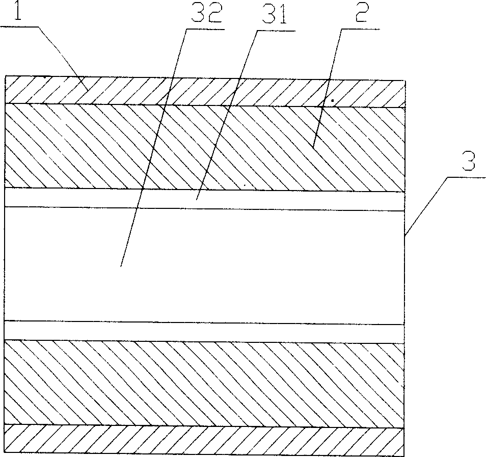
[0042] according to Figure 4 , a stacked structure of a twelve-layer printed circuit board is as follows: the sixth layer and the seventh layer are the power supply layer; the second layer, the fifth layer, the eighth layer, and the eleventh layer are the ground plane layer; the first layer The first, third, fourth, ninth, tenth, and twelfth layers are signal layers.
[0043] Depend on Figure 4 As shown, the fifth layer to the eighth layer are the ground plane layer G5, the power layer P6, the power layer P7, and the ground plane layer G8 in sequence. The power layer P6 and the power layer P7 are located in the middle stacking position of the printed circuit board. The stacked structure on the upper and lower sides of the power supply layers P6 and P7 is symmetrical, that is, the arrangement sequence from top to bottom is exactly the same as that from bottom to top, and the stacked structure is based on the power supply layers P6 and P7 as the axis of symmetry.
[0044] Th...
Embodiment 2
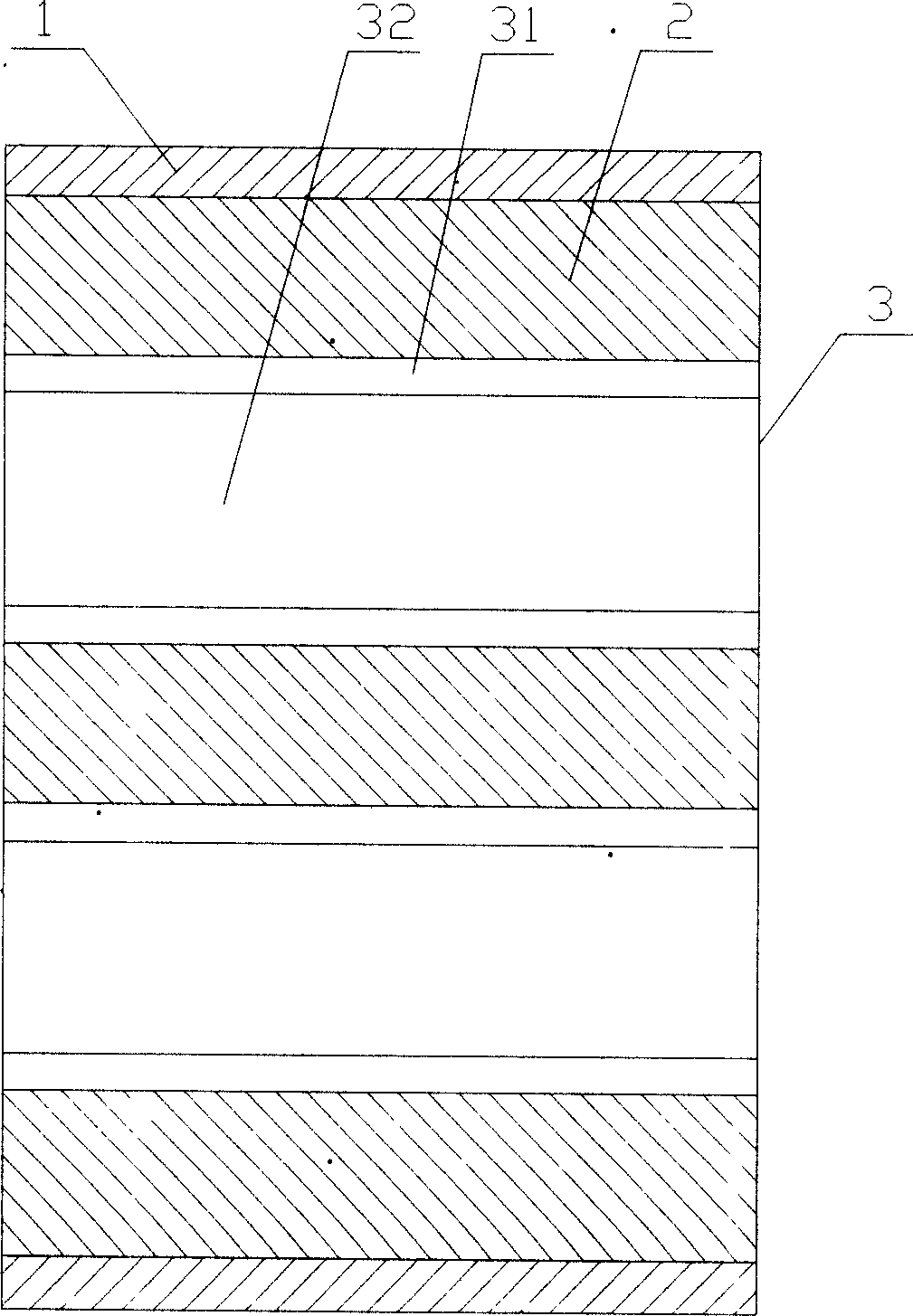
[0053] Such as Figure 5 A fourteen-layer printed circuit board is shown, and its laminated structure is: the seventh layer and the eighth layer are power supply layers; the second layer, the fourth layer, the sixth layer, the ninth layer, the eleventh layer, The thirteenth layer is the ground plane layer; the first, third, fifth, tenth, twelfth, and fourteenth layers are signal layers.
[0054] Depend on Figure 5 As shown, the sixth to ninth layers are the stacking sequence of the ground plane layer G6, the power layer P7, the power layer P8, and the ground plane layer G9, and the power layer P7 and the power layer P8 are located in the middle of the printed circuit board The stacking position, the upper and lower sides of the power layer P7 and P8 are symmetrical to the stacked structure, that is, the arrangement order from top to bottom is exactly the same as that from bottom to top, and the power layer P7 and P8 are the symmetry axes In the stacked structure, the signal...
Embodiment 3
[0066] according to Figure 6 , a sixteen-layer printed circuit board laminated structure is: the eighth layer, the ninth layer is the power layer; the second layer, the fifth layer, the seventh layer, the tenth layer, the twelfth layer, the fifteenth layer The first layer, the third layer, the fourth layer, the sixth layer, the eleventh layer, the thirteenth layer, the fourteenth layer, and the sixteenth layer are signal layers.
[0067] Depend on Figure 6 As shown, layers 7 to 10 include a stacking sequence of ground plane layer G7, power layer P8, power layer P9, and ground plane layer G10. Power layer P8 and power layer P9 are located in the middle of the printed circuit board The stacking position, the stacking structure of the upper and lower sides of the power supply layers P8 and P9 is symmetrical, that is, the arrangement order from top to bottom is exactly the same as that from bottom to top, and the stacking is based on the power supply layers P8 and P9 as the axi...
PUM
 Abstract
Description
Claims
Application Information