

Method and device for detecting ferro-electric film microwave dielectric property
A ferroelectric thin film and microwave dielectric technology, which is applied in measuring devices, testing dielectric strength, and measuring electricity, can solve problems such as insufficient resolution accuracy, achieve simple structure and principle, facilitate miniaturization, and facilitate device manufacturing and assembly Effect
- Summary
- Abstract
- Description
- Claims
- Application Information
AI Technical Summary
Problems solved by technology
Method used
Image

Examples
Embodiment 1
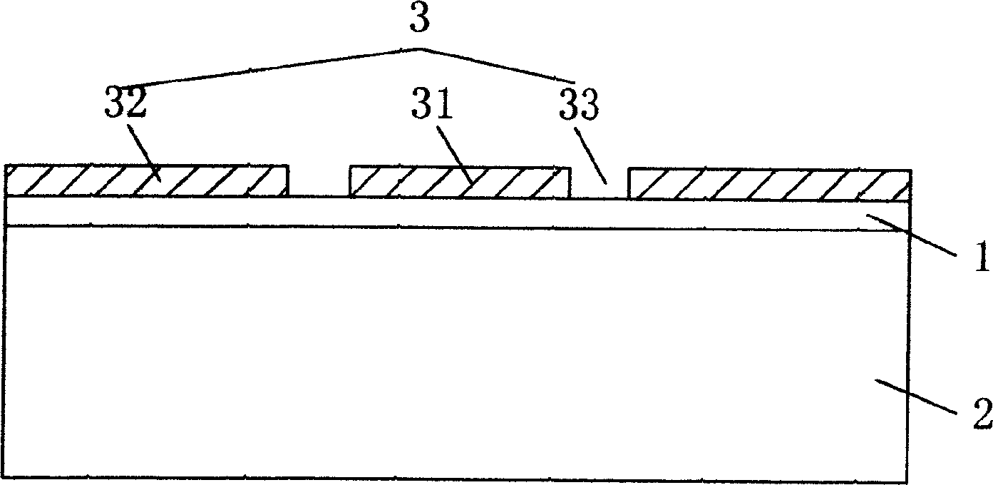
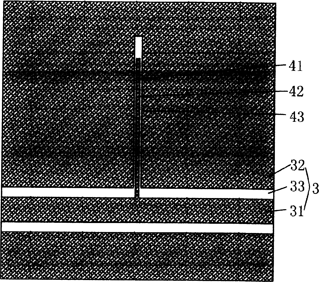
[0029] Utilize a square magnesium oxide substrate 2 with strontium barium titanate film 1 deposited on its surface, and plate a gold film with a thickness of more than 2.5 μm by magnetron sputtering, and the gold film forms a coplanar waveguide 3 and a coplanar open line 4, whose shape is as Figure 2a As shown, the coplanar waveguide 3 includes a main transmission line 31 and two ground planes 32 respectively located on both sides of the main transmission line. The cross-sectional view of the coplanar waveguide 3 is shown in figure 1 As shown, there is a slot 33 of equal width between the two ground planes 32 and the main transmission line 31. The 1 / 4 wavelength coplanar open line 4 is a straight line, and the coplanar open line 4 includes the transmission line 41 and the two sides of the transmission line respectively. The ground plane 43 separated by two gaps 42, the end of the transmission line 41 is an open end; the main transmission line 31 on the coplanar waveguide 3 is...
Embodiment 2
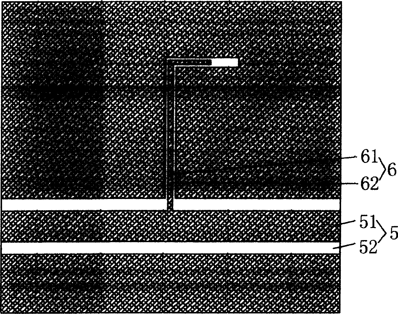
[0033] Lanthanum aluminate (LaAlO) with a barium titanate film deposited on a square surface 3 ) substrate, plated a gold film with a thickness of more than 2.5 μm by magnetron sputtering, the gold film forms a coplanar waveguide 5 and a 1 / 4 wavelength coplanar open line 6, and its shape is as follows Figure 2b As shown, the main transmission line 51 on the coplanar waveguide 5 is connected to the transmission line 61 on the 1 / 4 wavelength coplanar open line 6, the end of the transmission line 61 is an open end, and the 1 / 4 wavelength coplanar open line 6 is a broken line, The width of the slot 62 on it is not greater than 10 μm, and the width of the slot 52 on both sides of the main transmission line 51 on the coplanar waveguide 5 is 200 μm. The thickness of the barium titanate film is 0.3 μm. When the external voltage is applied to the barium titanate film through the device port, the electric field intensity at the gap 62 on the 1 / 4 wavelength coplanar open line is higher ...
Embodiment 3
[0036] Utilize a square aluminum oxide substrate deposited with barium strontium titanate film on the surface, and use magnetron sputtering to plate a copper film with a thickness of more than 2.5 μm. The copper film forms a coplanar waveguide with 7 and 1 / 4 wavelength coplanar Open line 8, the 1 / 4 wavelength coplanar open line 8 is a multiple folded line, its shape is as Figure 2c As shown, the main transmission line 71 on the coplanar waveguide 7 is connected to the transmission line 81 on the 1 / 4 wavelength coplanar open line 8, the end of the transmission line 81 is an open end, and the thickness of the barium strontium titanate film is 0.3 μm, 1 / The width of the slot 82 on the 4-wavelength coplanar open line 8 is not greater than 5 μm, and the width of the slot 72 on both sides of the main transmission line 71 of the coplanar waveguide 7 is 200 μm. When the external voltage is applied to the barium strontium titanate film through the device port, the electric field inte...
PUM
| Property | Measurement | Unit |
|---|---|---|
| Seam width | aaaaa | aaaaa |
Abstract
Description
Claims
Application Information