Isolation spacer for thin isolation semiconductor

A technology of semiconductors and components, applied in the field of microelectronic components with thin insulating semiconductor structures

Inactive Publication Date: 2006-04-26
TAIWAN SEMICON MFG CO LTD
View PDF0 Cites 3 Cited by
  • Summary
  • Abstract
  • Description
  • Claims
  • Application Information

AI Technical Summary

Problems solved by technology

In the subsequent metal silicide process, metal silicide residues will form in the undercut area and cause leakage with the adjacent channel area

Method used


Image

  • Isolation spacer for thin isolation semiconductor
  • Isolation spacer for thin isolation semiconductor
  • Isolation spacer for thin isolation semiconductor

Examples


Embodiment Construction

[0033] The following discussion provides quite a few embodiments or examples to incorporate different features in different embodiments. Specific examples of components and arrangements are described below to simplify the disclosure. Therefore, mere few examples should not be considered limiting. Additionally, the same notation and text may be used in different instances throughout the disclosure. Reuse of symbols and text is for simplification and clarity only and does not dictate relationships between different embodiments and / or discussion outlines.

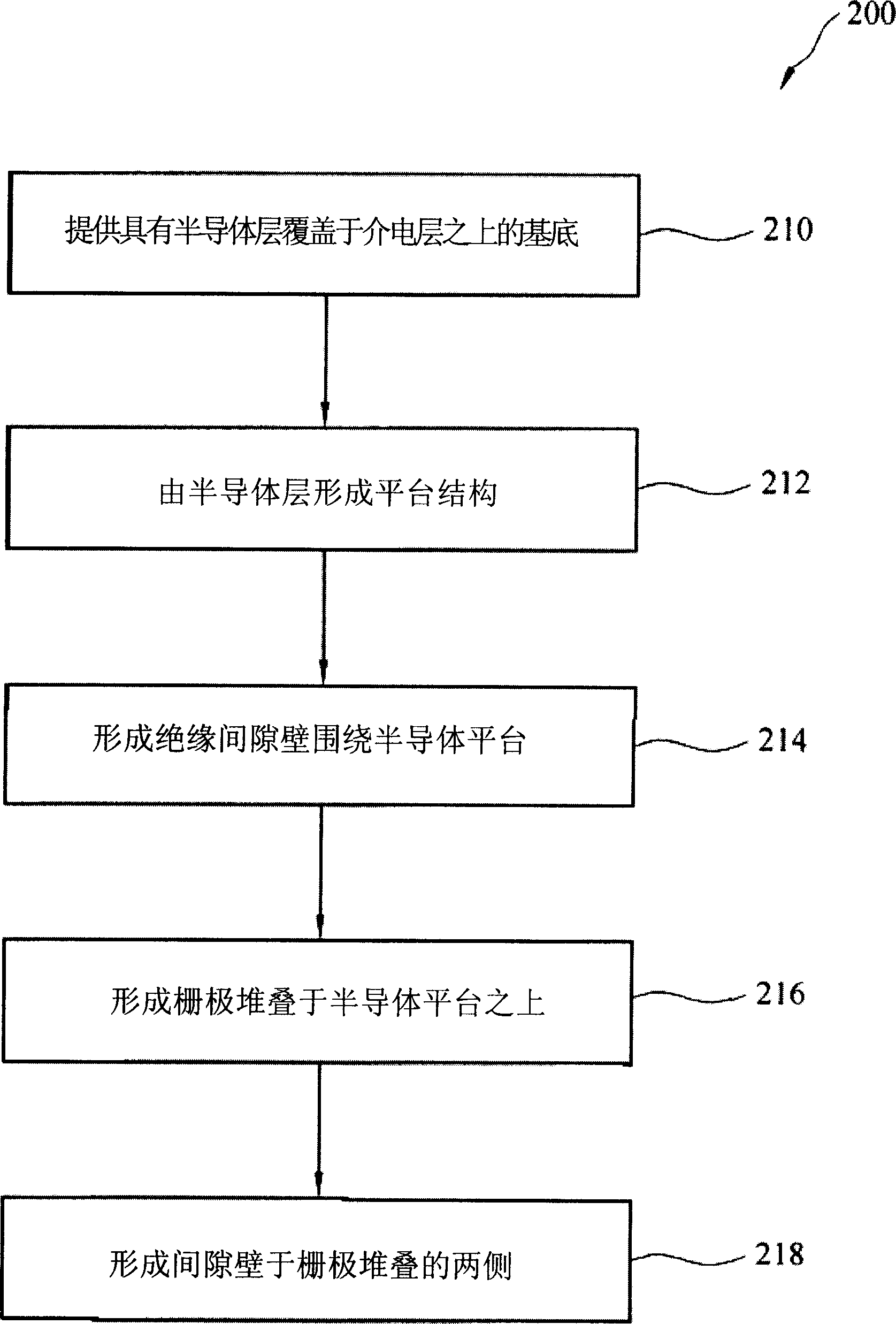
[0034] figure 1 is a simplified flowchart of the method 200 for forming a thin insulating semiconductor device. and Figure 2 to Figure 7a and 7b are schematic cross-sectional views of the process of forming the semiconductor device 100 .

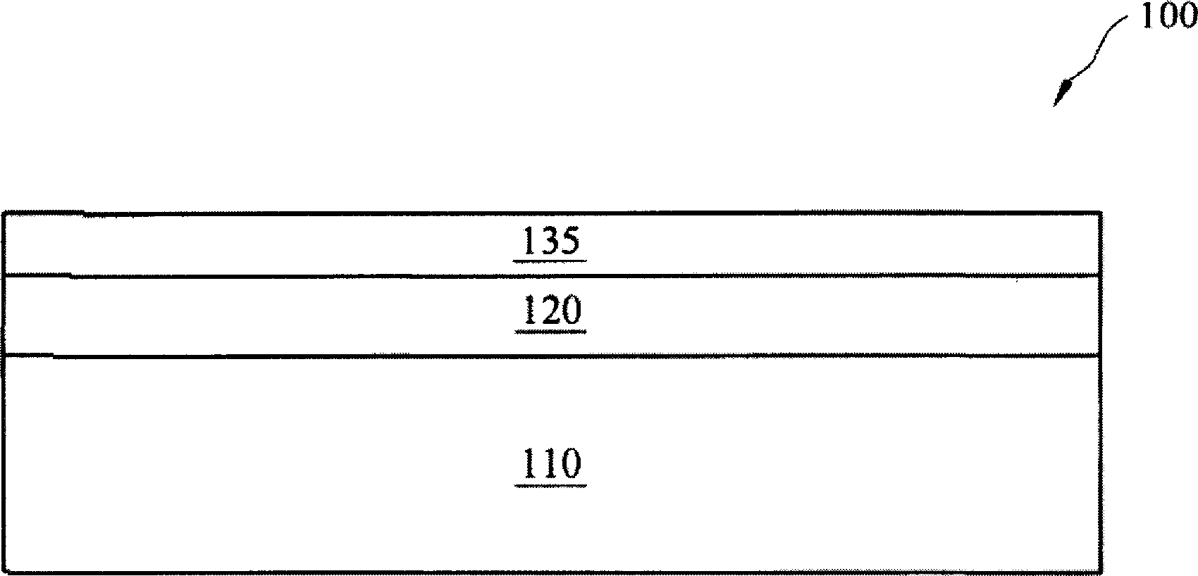
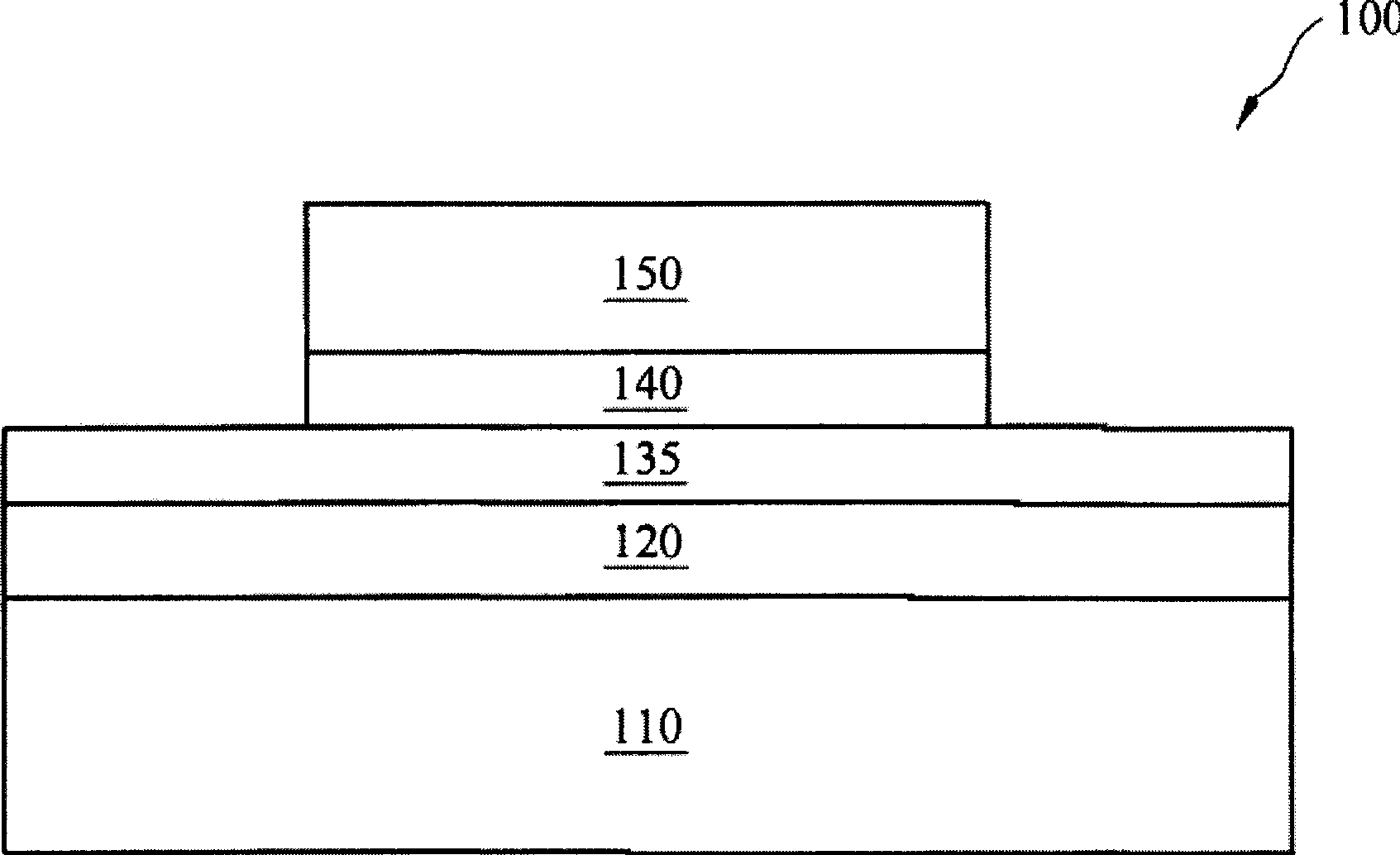
[0035] Method 200 starts from step 210, first provides as figure 2 A semiconductor substrate 110 is shown, a dielectric layer 120 is formed on the substrate 110 , and a semiconductor...


PUM


Abstract

A semiconductor device includes a semiconductor platform on a dielectric layer; a gate stack formed on the semiconductor platform; and an insulating spacer formed around the semiconductor platform and filling an undercut area at the edge of the semiconductor platform.

Description

technical field [0001] The present invention relates to a microelectronic component, and in particular to a microelectronic component with a thin insulating semiconductor structure. Background technique [0002] When thin semiconductor on insulator (Semiconductor On Insulator, SOI) is used to manufacture semiconductor microelectronic components, the etching and cleaning processes when patterning the gate stack will form undercuts in the buried insulating layer. In the subsequent metal silicide process, metal silicide residues will be formed in the undercut region and cause leakage with adjacent channel regions. Contents of the invention [0003] In order to solve the leakage problem caused by the known thin insulating semiconductor technology, the present invention discloses a semiconductor element, comprising a semiconductor platform located on a dielectric layer; a gate stack located on the semiconductor platform; an insulating spacer surrounding the semiconductor platfo...

Claims


Application Information

Patent Timeline
Patent Type & Authority Applications(China)
IPC IPC(8): H01L29/78H01L27/12
CPCH01L27/1203H01L29/66772H01L29/78618Y10S257/90
Inventor 柯志欣李文钦杨育佳葛崇祜
Owner TAIWAN SEMICON MFG CO LTD
Why Eureka
Try Eureka