Optical sensor

A technology of light sensor and photoelectric device, applied in the field of light sensor

Inactive Publication Date: 2006-05-31
PANASONIC CORP
View PDF1 Cites 8 Cited by
  • Summary
  • Abstract
  • Description
  • Claims
  • Application Information

AI Technical Summary

Problems solved by technology

[0009] However, it is difficult to obtain a stable focus error signal and a stable tracking signal from two light sources at the same time in conventional techniques

Method used


Image

  • Optical sensor
  • Optical sensor
  • Optical sensor

Examples


no. 1 example

[0047] The photosensor according to the first embodiment has two light-emitting elements, and can obtain a focus error signal and a tracking error signal with high stability by using a holographic optical element having four regions whose characteristics are different from each other.

[0048] (1) The structure of the light sensor

[0049] First, the structure of the photosensor according to the first embodiment will be described.

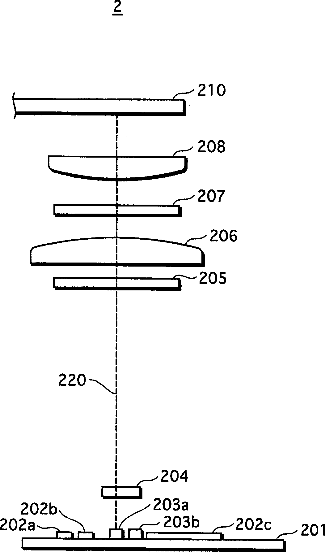
[0050] figure 2 is a sectional view schematically showing the structure of the photosensor according to the first embodiment of the present invention.

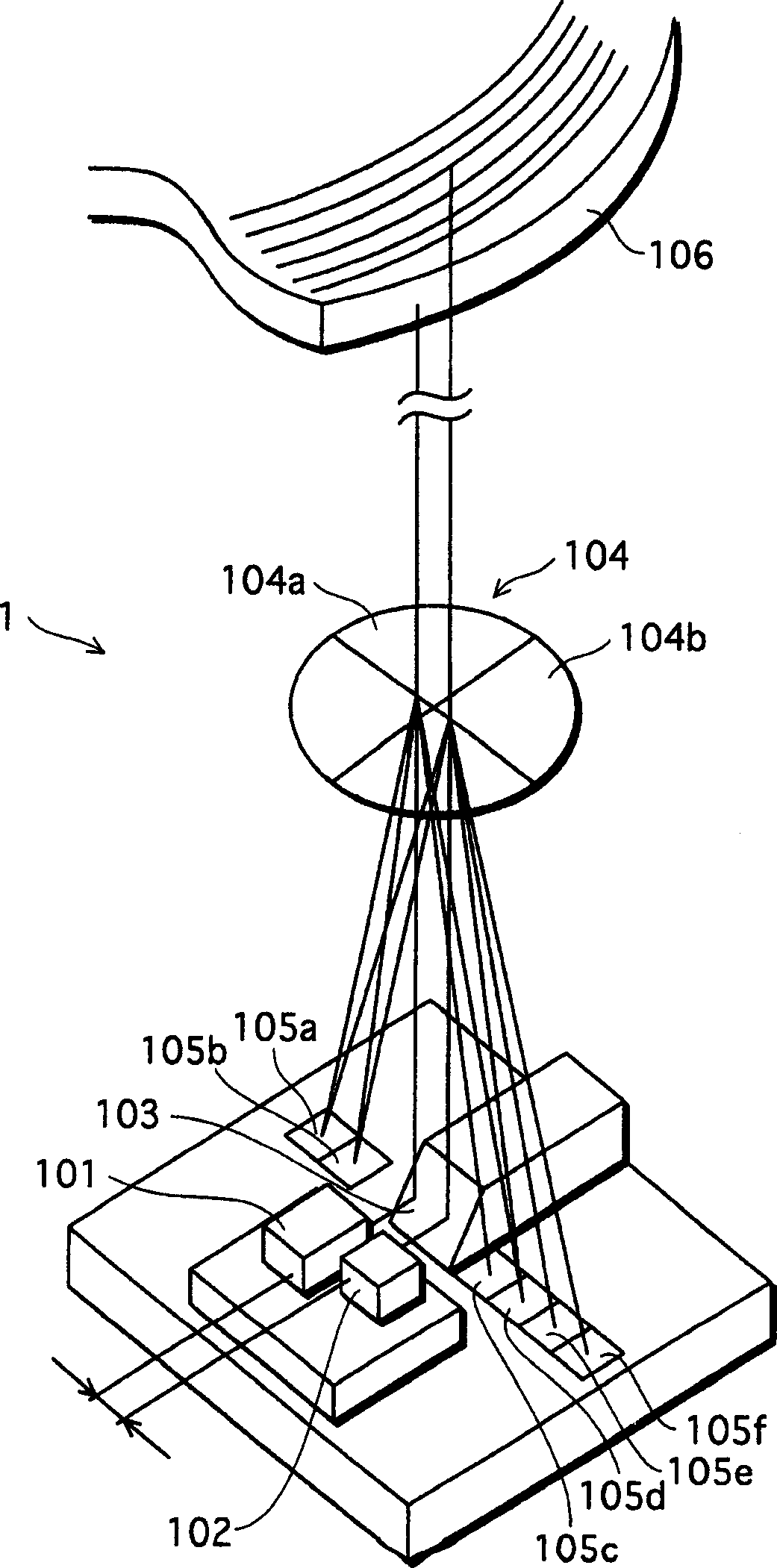
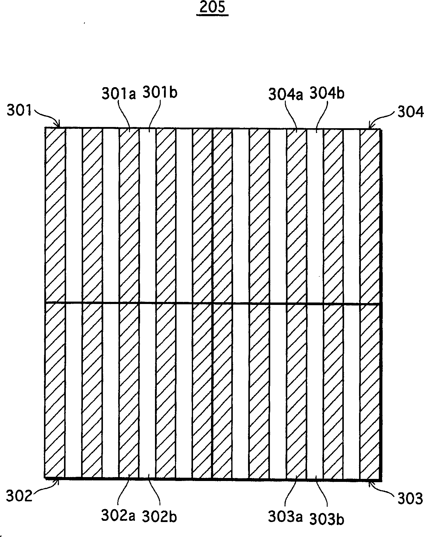
[0051] Such as figure 2 As shown, the optical sensor 2 includes an IC substrate 201, photoelectric device groups 202a to 202c, laser diodes 203a and 203b, a diffraction grating 204, a holographic optical element 205, a collimating lens 206, a quarter retardation plate 207 and an objective lens 208. The optical sensor records information on the optical recording medium 210 or reproduces informa...

no. 3 example

[0123] Next, a third embodiment of the present invention will be described. The photosensor according to the third embodiment has almost the same structure as that of the photosensor according to the first embodiment, but the structure of the diffraction grating is different. The main differences are described below.

[0124] First, the structure of the photosensor is described. Figure 9 is a sectional view schematically showing the structure of an optical sensor according to a third embodiment of the present invention. Such as Figure 9 As shown, just like the above-mentioned photosensor 2 according to the first embodiment, the photosensor 9 includes an IC substrate 901, photoelectric device groups 902a to 902c, laser diodes 903a and 903b, a holographic optical element 905, a collimator lens 906, 1 / 4 retardation plate 907 and objective lens 908, and additionally includes a diffraction grating plate 904 and a package 909.

[0125] The package 909 has a cylindrical shape ...

no. 4 example

[0131] Next, a fourth embodiment of the present invention will be described. The photosensor according to the fourth embodiment has almost the same structure as that of the photosensor according to the first embodiment, but the structure of the light-emitting element is different. The main differences are described below.

[0132] Figure 10 is a sectional view schematically showing the structure of a photosensor according to a fourth embodiment of the present invention. Such as Figure 10 As shown, the optical sensor 10 includes an IC substrate 1001, photoelectric device groups 1002a to 1002c, a laser diode 1003, a diffraction grating 1004, a holographic optical element 1005, a collimating lens 1006, a quarter retardation plate 1007 and an objective lens 1008.

[0133] The laser diode 1003 according to the fourth embodiment of the present invention is a monolithic dual-wavelength laser diode in which two laser diodes are integrated.

[0134] The positional relationship be...


PUM


Abstract

The light sensor includes: two laser diodes, which are used to emit light beams with different wavelengths; a diffraction grating, which is used to diffract each light beam into a zero-order diffraction beam and a positive and negative first-order diffraction beam; a holographic optical element, which is used to diffract from a light beam reflected by the recording medium; and a photoelectric device for receiving the light beam diffracted by the holographic optical element, wherein the photoelectric device for generating a tracking error signal and the photoelectric device for generating a focus error signal are arranged opposite to the laser diode side so as to face each other.

Description

technical field [0001] The present invention relates to an optical sensor for recording and reproducing information on an optical recording medium, which uses light of different wavelengths for recording and reproducing. In particular, the present invention relates to a technique for acquiring a focus error signal and a tracking error signal with high stability. Background technique [0002] Cross References to Related Applications [0003] This application is based on Application No. 2004-283890 filed in Japan, and thus the contents of this application are incorporated by reference. [0004] In recent years, optical recording media such as CDs (Compact Discs) and DVDs have become widely popular. Optical recording media record and reproduce data using light of different wavelengths (for example, 780nm to 820nm for CDs, and 635nm to 680nm for DVDs). In consideration of user convenience, it is preferable that an optical sensor is capable of recording and reproducing data on...

Claims


Application Information

Patent Timeline
Patent Type & Authority Applications(China)
IPC IPC(8): G11B7/09G11B7/12G11B7/13G11B7/135
CPCG11B7/0903G11B7/123G11B7/131G11B7/1353G11B2007/0006G11B7/09
Inventor 西本雅彦河内泰之井岛新一奥田拓也小野将之
Owner PANASONIC CORP
Why Eureka
Try Eureka