
Patsnap Eureka
For R&D, Patsnap Eureka makes reading and utilizing patents & technical documents easy.
Patsnap Eureka AIR
Designed for self-driven R&D workflows. Generate viable solutions, solve complex R&D challenges, empower your innovation with AI.

Patsnap Eureka Materials
Designed for material experts only. Revolutionize your material R&D, from search, analyze, to developing new materials.

TechResearch
Generate reliable direction feasibility study reports for your R&D in just a few steps.

TechSeek
Discover and master advanced knowledge NOW. Basics, ideas, possibilities, all at once.

TechMind
As an expert in R&D Theories, TechMind can generates customized viable solutions instantly.

TechRisk
Analyze your overall solution with one click, know your potential R&D risks in advance.

TechMonitor
Get weekly tech updates, stay abreast of the latest tech innovations and key insights.
Quickflashing memory unit manufacturing method
A storage unit and manufacturing method technology, applied in semiconductor/solid-state device manufacturing, electrical components, circuits, etc., can solve problems such as influence, poor quality of gate oxide layer, and limitation of surface cleaning steps
- Summary
- Abstract
- Description
- Claims
- Application Information
AI Technical Summary
Problems solved by technology
Method used
Image

Examples
Embodiment Construction
[0015] The method of the present invention will be described in detail according to the following preferred embodiment and with reference to the accompanying drawings.
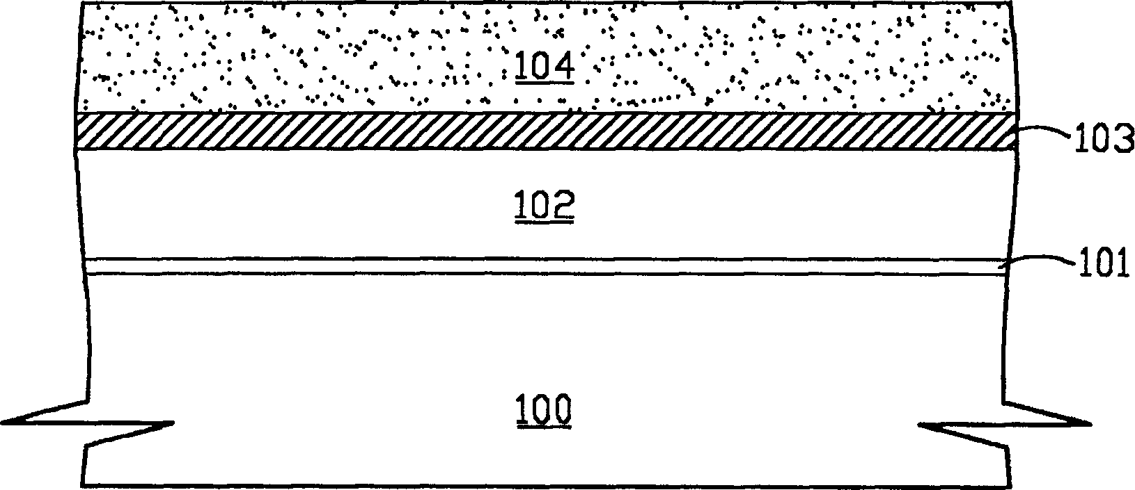
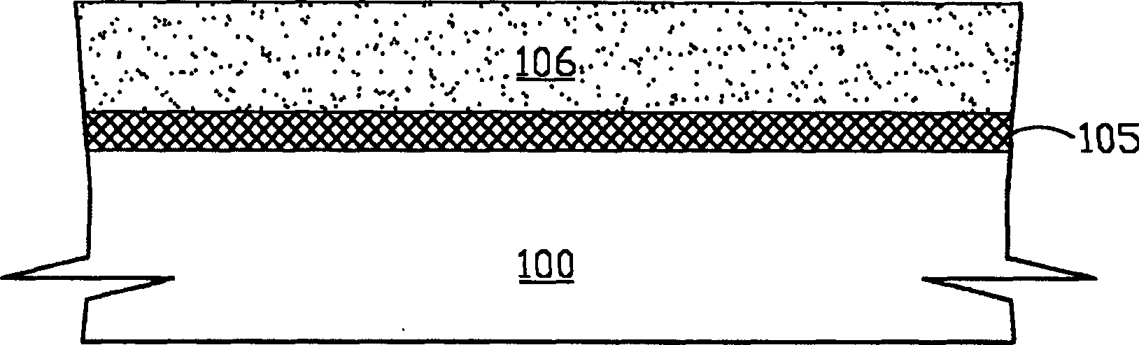
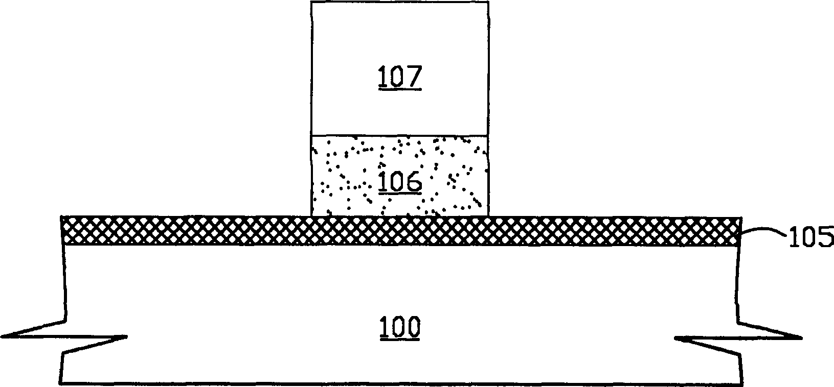
[0016] A preferred embodiment of the invention is shown in Figure 1A to Figure 1D and Figure 2A to Figure 2E ,in Figure 1A to Figure 1D It is a schematic cross-sectional view of various formation steps of the peripheral region (periphery region) of the flash electrically erasable and programmable read-only memory unit of the present invention, and Figure 2A to Figure 2E It is a schematic cross-sectional view of various formation steps of the memory cell region of the flash electrically erasable and programmable read-only memory unit of the present invention.
[0017] refer to Figure 1A and Figure 2A , a tunnel oxide layer 101 is formed on a semiconductor substrate 100 with a first conductivity. The semiconductor substrate 100 can be an N-type or P-type substrate, preferably a P-type silicon substrate....
PUM
 Abstract
Description
Claims
Application Information
 - R&D Engineer
- R&D Manager
- IP Professional
- Industry Leading Data Capabilities
- Powerful AI technology
- Patent DNA Extraction
Browse by: Latest US Patents, China's latest patents, Technical Efficacy Thesaurus, Application Domain, Technology Topic, Popular Technical Reports.
© 2024 PatSnap. All rights reserved.Legal|Privacy policy|Modern Slavery Act Transparency Statement|Sitemap|About US| Contact US: help@patsnap.com