USB applier

An application module and corresponding technology, applied in the direction of the coupling device, the two-part connection device, the components of the connection device, etc., can solve the problems of work efficiency and functional limitations, waste, insufficient data transmission lines, etc., and achieve higher signal transmission frequency. Wide and transmission speed, increase work efficiency and function, reduce the effect of overall volume

Inactive Publication Date: 2006-08-16
INNODISK CORP
View PDF0 Cites 8 Cited by
  • Summary
  • Abstract
  • Description
  • Claims
  • Application Information

AI Technical Summary

Problems solved by technology

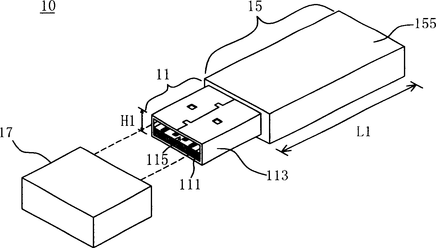
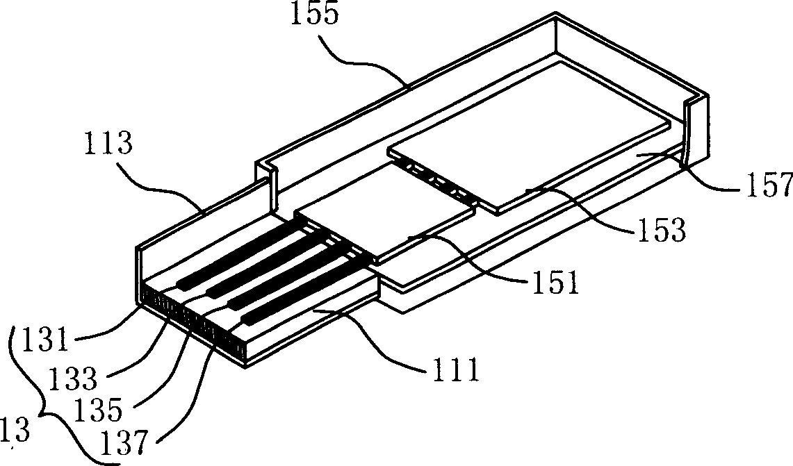
[0006] In the above-mentioned existing USB application device 10, the carrying plate 111 is a solid resin material, and its only function is to carry and fix the USB connection terminal 13, but it occupies a relatively large volume of the USB connection head 11, relatively It is also difficult to reduce the volume or length of the USB application device 10, so in terms of the production cost and portability of the USB application device 10, a considerable degree of waste and inconvenience are caused.
[0007] In the existing USB connector 11, the top surface of the carrier board 111 only has a VCC power supply line 131, a GND power supply line 137, a D+ transmission line 133 and a D- transmission line 135, and its data transmission line is obviously insufficient, so , its work efficiency and functions are also limited, and it cannot meet the requirements of the information age for the efficiency and functions of information products
[0008] The protective cover 17 of the existing USB application device 10 is fixed on the outer surface of the USB connector 11 in the form of a cover. Although this fixing method can achieve the purpose of protecting the USB connector 11, it also increases the USB application device 10. overall volume
[0009] At the same time, the existing USB connector 11 and the USB shell layer 155 are made of different materials. Therefore, in the manufacturing process, the two must be made separately and then bonded, which not only increases the complexity of the manufacturing, but also makes the bonding process difficult. If the bonding effect is not good, there will be shaking between the USB connector 11 and the USB shell layer 155, which will cause damage to the internal connection lines of the USB application device 10 after long-term use.

Method used


Image

  • USB applier
  • USB applier
  • USB applier

Examples


Embodiment Construction

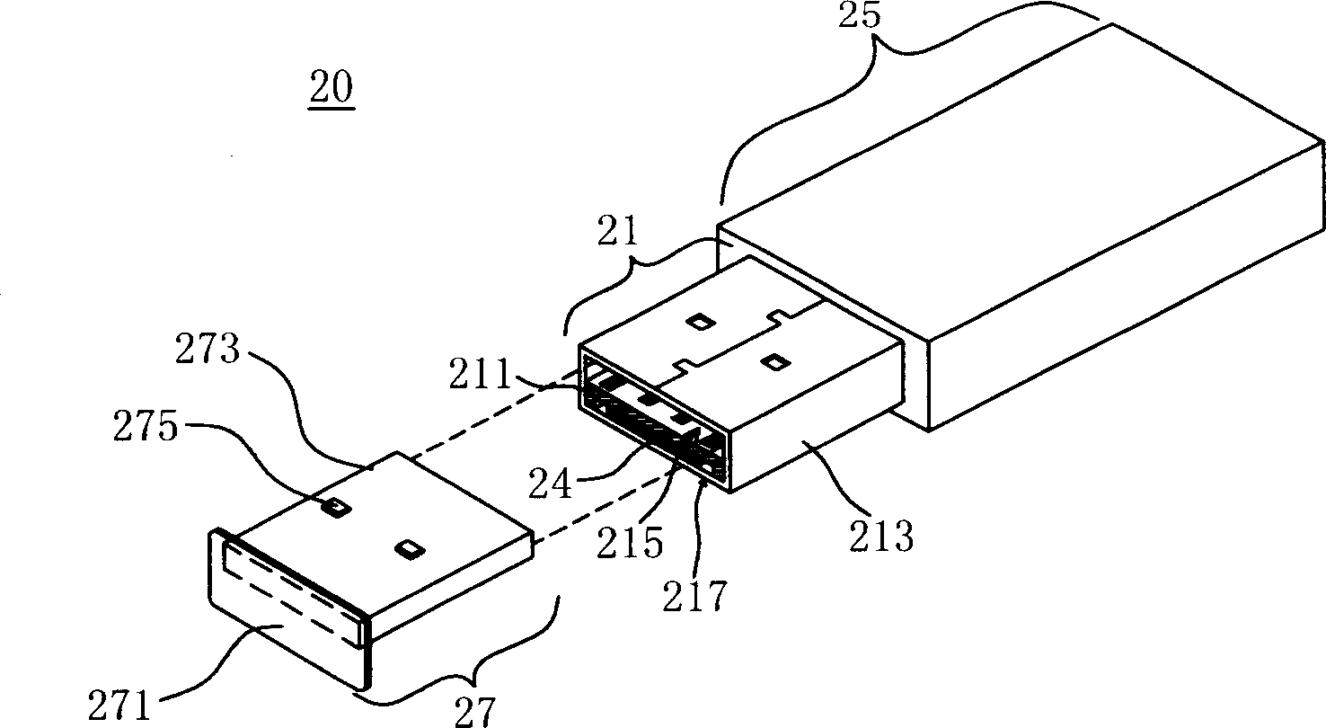
[0065] Such as image 3 and Figure 3A As shown, the USB application device 20 of the present invention, such as mobile hard disk, Bluetooth, digital camera, MP3 player, control circuit, GPS, recording pen, TV viewing module or wireless network card module and other devices, its front end is provided with a connector (Series A Plug) 21, the rear end of the connector 21 is connected with a USB electronic application module 25. Wherein, the shell layer 213 of the connector 21 encloses a PCB carrier board 211 made of a PCB circuit board, and a connecting interlayer 215 can be naturally formed between the top surface of the PCB carrier board 211 and the outer shell layer 213, the connecting interlayer 215 can be plugged with another connection socket (Series A receptacle), and the top surface of the PCB carrier board 211 in the connection interlayer 215 can carry a plurality of first connection terminals 23 electrically connected to the electronic application module 25 . When th...


PUM


Abstract

A printed circuit board (PCB) is taken as USB port bearing board. On the surface of PCB bearing board, multi first connection ports can be mounted. A bottom interlayer is formed between the bottom surface of PCB bearing board and outer shell of connector, and is used to mount at least one electronic component by which the length of USB module can be shortened or working efficiency and functionality of USB module can be improved. And meanwhile, at part of the top surface not having first connection ports at least one board-top data transmission line can be installed.

Description

technical field [0001] The present invention relates to a USB application device, in particular to an improved structure using a PCB circuit board as an internal bearing board of a connector, which can not only reduce the length of the USB application device, but also effectively improve the working efficiency and functions of the USB application device . Background technique [0002] The USB (Universal Serial Bus) transmission interface is widely used in various computer peripheral devices, information appliances (IA) or 3C consumer electronics products due to its advantages of convenience, expandability and high transmission speed. , is an indispensable transmission interface tool in people's work and family life today. [0003] The existing USB device terminal structure is as follows: figure 1 and figure 2 As shown, a USB application device 10 with a USB connector 11 (Series A Plug), such as an MP3 player or a recorder, etc., has a USB connector 11 at its front end, a...

Claims


Application Information

Patent Timeline
Patent Type & Authority Applications(China)
IPC IPC(8): H01R13/66H01R24/06
Inventor 李钟亮林传生蔡瑞隆
Owner INNODISK CORP
Why Eureka
Try Eureka