Organic electroluminescence display and its producing method

A technology for electroluminescent display and manufacturing method, which is applied in the direction of electroluminescent light source, electric light source, light source, etc. It can solve the problems of affecting the yield rate, unstable short circuit or potential short circuit, waste of integrated circuit driver chips, etc., so as to avoid waste , Improve yield rate and reduce production cost

Active Publication Date: 2006-08-23
TRULY SEMICON
View PDF0 Cites 16 Cited by
  • Summary
  • Abstract
  • Description
  • Claims
  • Application Information

AI Technical Summary

Problems solved by technology

The structure of an organic electroluminescent display device is a multi-layer organic or inorganic thin film functional layer sandwiched between the anode and the cathode. The total thickness of the film is about 50-500 nanometers. Pollution is inevitable. Therefore, internal defects of the device caused by tiny impurities are also unavoidable, and impurities such as tiny dust are sandwiched between the cathode and anode electrodes or there are pinholes in the film, which can easily cause organic electroluminescence. Display device negative and pos

Method used


Image

  • Organic electroluminescence display and its producing method
  • Organic electroluminescence display and its producing method
  • Organic electroluminescence display and its producing method

Examples


Embodiment 1

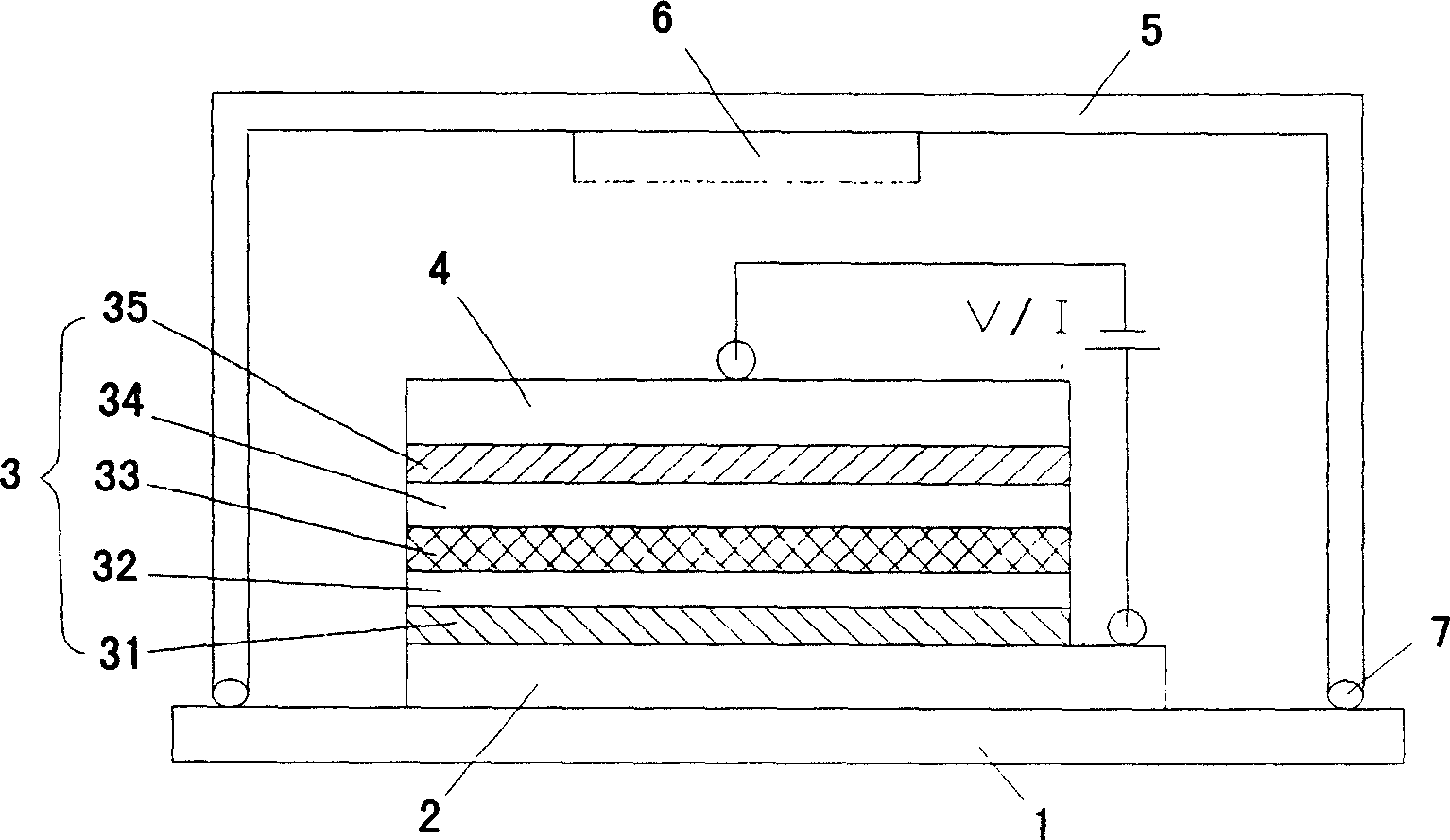
[0048] Embodiment 1. Aging by constant forward current: a forward current is applied continuously for 30 minutes, and the current density is 2.5 mA / cm2.

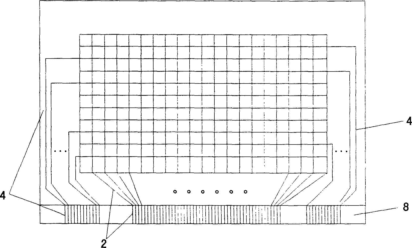
[0049] 96 organic electroluminescent devices were produced. After aging with forward current, 6 grains of negative and positive electrode short-circuit defects were detected, accounting for 6.25%. 24 modules were bonded by adding an integrated circuit driver chip. During the aging process of the modules, 12 short circuits were detected between the positive and negative electrodes, accounting for 50%.

Embodiment 2

[0050] Embodiment 2: Aging by combination of forward pulse and reverse pulse: apply a forward current with a current density of 160mA / cm2 for 15.6ms continuously, and then apply a reverse voltage -20V with a frequency of 1Hz for 984.4ms continuously, for a total of 30 minutes.

[0051] 144 organic electroluminescent devices were produced. After using combined pulse aging, 11 grains of negative and positive electrode short-circuit defects were detected, accounting for 7.64%. 27 modules were bonded by adding integrated circuit driver chips, and 1 module was found to be short-circuited between the positive and negative electrodes during the aging process of the modules, accounting for 3.7%.

Embodiment 3

[0052] Embodiment 3. Aging by constant forward current: applying a forward current with a current density of 2.5 mA / cm2 for 4 hours continuously.

[0053] 432 organic electroluminescent devices were produced. During the aging process, a total of 32 short-circuit defects appeared, one of which was eliminated, accounting for 3.1% of the short-circuit defects, and the remaining 31 short-circuit defects appeared, accounting for 7.18% of the total. 344 modules were bonded by adding integrated circuit driver chips, and 144 short-circuit defects of positive and negative electrodes were detected during the aging process of the modules, accounting for 41.86%. In general, the defective rate of negative and positive electrode short circuit accounted for 40.51% of the total.


PUM

PropertyMeasurementUnit
Pulse widthaaaaaaaaaa

Abstract

Said invention discloses organic electroluminescent display and manufacture method. It contains applying forward voltage (current pulse), reverse voltage pulse or both of them between anode and cathode of display device before packaging organic electroluminescent display device or in aging, partial short circuit fault instant burning-out or partial diode characteristic broken down instead of presenting short circuit phenomena and to make unstabilized short circuit fault speeding up representation for taking out as unqualified product. Said invented method can effectively inspect even eliminate short circuit fault before bonding electroluminescent display device and integrated circuit driving chip, raising non-defective rate and greatly reducing production costs.

Description

technical field [0001] The invention relates to an organic electroluminescent display and a manufacturing method thereof, in particular to an aging inspection method for inspecting or even eliminating short-circuit defects of negative and positive electrodes in organic electroluminescent display devices during the manufacturing process of the organic electroluminescent display. Background technique [0002] Since C.W.TANG et al. of KODAK Corporation of the United States released a low-voltage drive, high luminous efficiency, and high luminous brightness in 1987, organic electroluminescent devices (Organic Electroluminescent Devices, referred to as OLED devices), organic electroluminescent display devices Research work has made a breakthrough. After nearly 20 years of research and development, organic electroluminescent display device technology has made great progress. With the continuous maturity of equipment, materials, processes and other technologies, organic electrolumi...

Claims


Application Information

Patent Timeline
IPC IPC(8): H05B33/10H05B33/00G01R31/28
Inventor 苏君海陈升东黄学男苏初榜张色冯
Owner TRULY SEMICON
Why Eureka
Try Eureka