Semiconductor wafer carrier mapping sensor

A wafer carrier and sensor technology, used in semiconductor/solid-state device manufacturing, instrumentation, scattering characteristic measurement, etc., to solve problems such as insufficient registration of dark wafers, false cross slot errors, and poor detection of dark wafers

Inactive Publication Date: 2006-09-13
CYBEROPTICS SEMICON
View PDF0 Cites 4 Cited by
  • Summary
  • Abstract
  • Description
  • Claims
  • Application Information

AI Technical Summary

Problems solved by technology

Conversely, when the system is optimally tuned for bright wafers, dark wafers may not register well enough to make their presence known
Disadvantageously, tuning the sensing system to compromise between these two extremes necessarily creates a worse case where false cross-slot errors still occur and some dark wafers are not detected at all

Method used


Image

  • Semiconductor wafer carrier mapping sensor
  • Semiconductor wafer carrier mapping sensor
  • Semiconductor wafer carrier mapping sensor

Examples


Embodiment Construction

[0012] Embodiments of the invention relate to increasing the effective dynamic range of laser-based wafer carrier mapping sensors. Various features and combinations thereof have been explored, synergistically providing significantly advanced wafer inspection. These features will be elucidated separately below, but it should be clearly understood that embodiments of the invention are not limited to individual features, but also include vast permutations of combinations thereof.

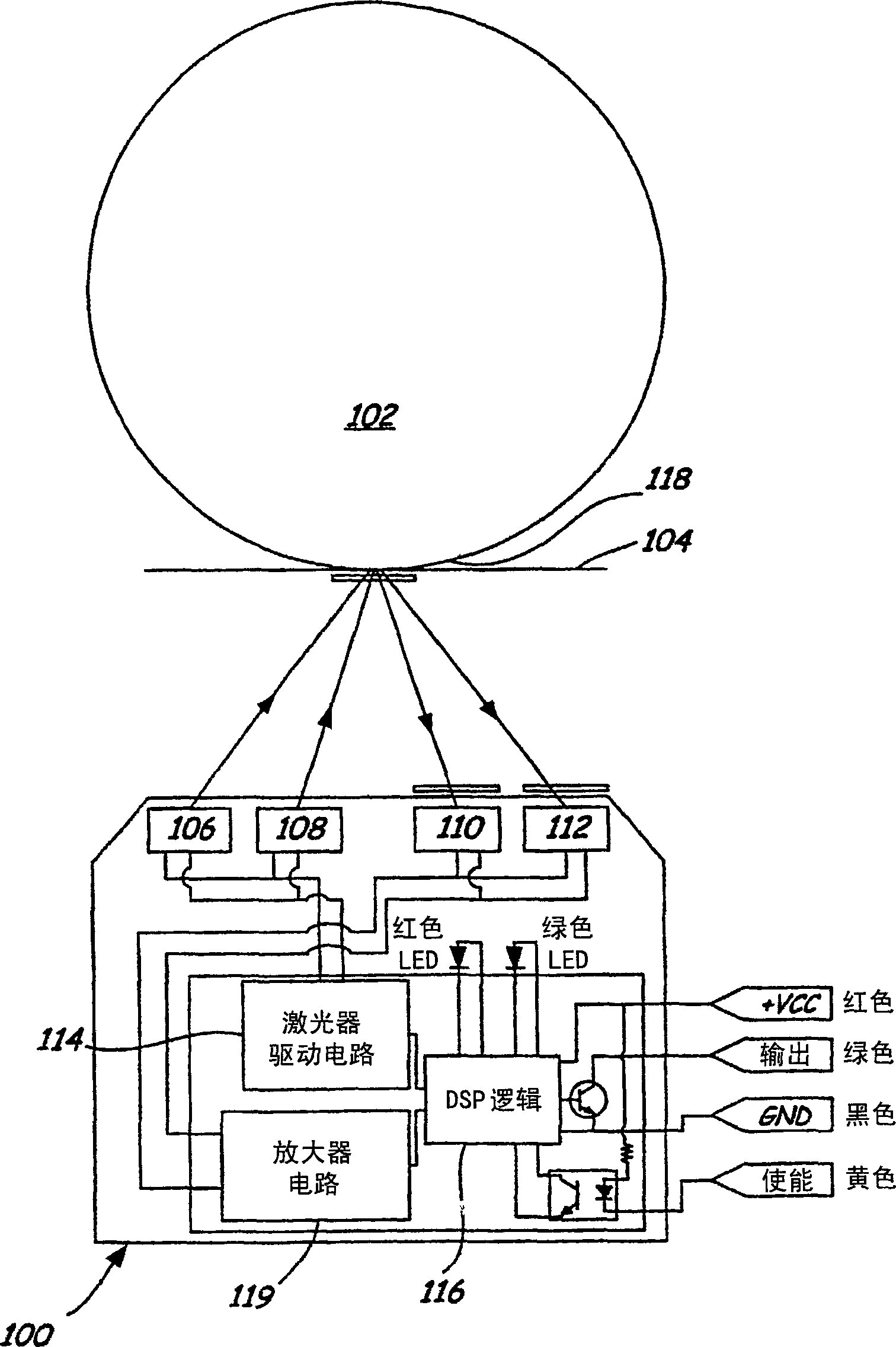
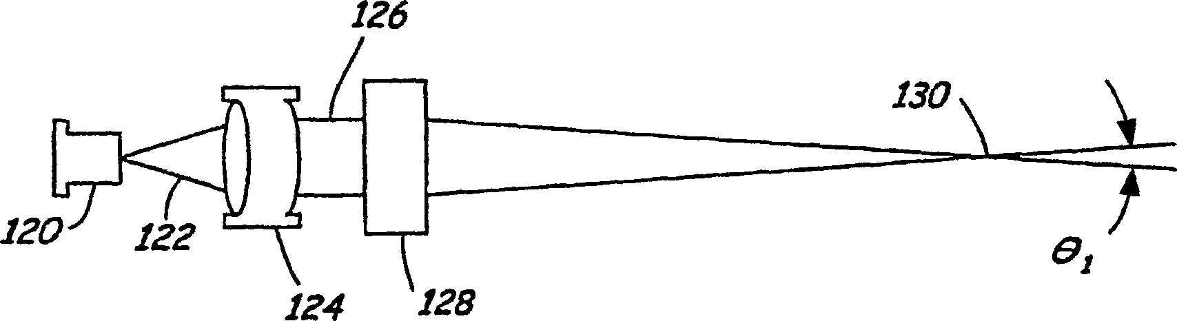
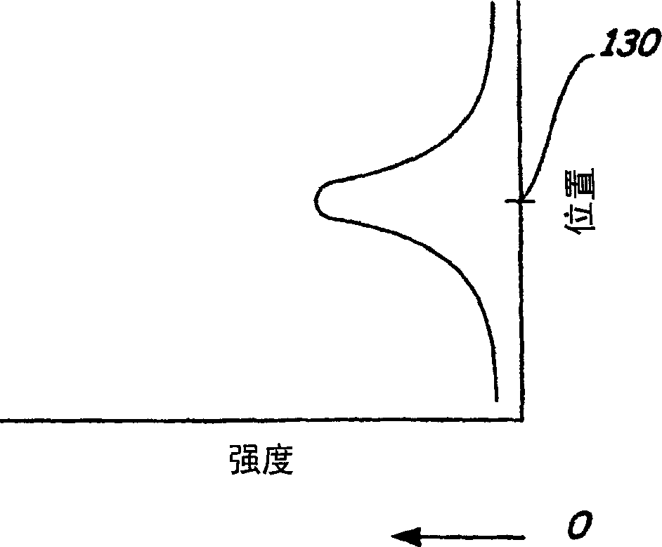
[0013] figure 1 is a schematic diagram of a wafer carrier mapping system according to an embodiment of the invention. Figure 2 shows a more optimized sensor geometry for on-axis applications. Sensor 100 is configured to detect a wafer, such as wafer 102 in carrier 104 . One example of carrier 104 is a front opening unified container (FOUP). When reflected from a wafer edge 118, two laser light sources 106 and 108, preferably laser diodes, shine into detectors 110 and 112, respectively. Each laser ...


PUM

PropertyMeasurementUnit
lengthaaaaaaaaaa
diameteraaaaaaaaaa
wavelengthaaaaaaaaaa

Abstract

An improved laser-based wafer carrier mapping sensor (100) is provided. The sensor (100) includes a number of improvements including laser source improvements; optical improvements; and detector improvements. Laser source (106, 108) improvements include the type of laser sources used as well as the specification of size and power of such sources (106, 108). Optical improvements include features that intentionally defocus the laser stripe on the wafer (102) as well as additional features that help ensure precision stripe generation. Detector improvements include increasing gain while decreasing the effects of ambient light. Various combinations of these features provide additional synergies that facilitate the construction of a sensor (100) with significantly improved dynamic response while decreasing the frequency of false cross slot errors.

Description

technical field [0001] The present invention relates to a semiconductor wafer carrier mapping sensor. Background technique [0002] Wafer carrier mapping sensors are used in the manufacture and handling of semiconductor wafers in order to detect wafers in wafer carriers. In order to efficiently process wafers in a carrier, a semiconductor tool must know which locations within the carrier have wafers and whether they are properly held therein. Wafer carrier mapping sensors scan the wafer edge to detect wafer presence / absence, and other errors such as cross grooves. "Cross grooves" are wafer position errors in which a wafer is not held in a single "groove" but mistakenly straddles a pair of grooves. In this case, mainly, the tool does not try to interact with the wafer, and an error occurs. [0003] Wafer carrier mapping systems have begun to face difficult challenges recently created by the increasing use of dark wafers, typically with nitride coatings. While the mapping ...

Claims


Application Information

Patent Timeline
Patent Type & Authority Applications(China)
IPC IPC(8): H01L21/00G01N21/55G01B11/00H01L21/67H01L21/673
CPCH01L21/67265H01L21/6735H01L21/68
Inventor 费利克斯·J·舒达
Owner CYBEROPTICS SEMICON
Why Eureka
Try Eureka