
Method of producing a colour display device and colour display device

An equipment and liquid crystal display technology, applied in optics, instruments, nonlinear optics, etc., can solve the problems of increasing final products, time-consuming batch processes, complexity, etc., and achieve the effect of improving efficiency and reducing manufacturing costs

Inactive Publication Date: 2006-09-27
KONINKLIJKE PHILIPS ELECTRONICS NV
View PDF2 Cites 7 Cited by
  • Summary
  • Abstract
  • Description
  • Claims
  • Application Information

AI Technical Summary

Problems solved by technology

[0009] The disadvantage of this method is that it is a complex and time-consuming batch process
For example, the second substrate must be fitted with spacer elements, and the interstitial regions must be filled with nematic LC material, which is particularly time-consuming for large multicolor LCDs, increases the cost of the manufacturing process, and increases the cost of the final product. , that is, the cost of multi-color LCD

Method used


Image

  • Method of producing a colour display device and colour display device
  • Method of producing a colour display device and colour display device
  • Method of producing a colour display device and colour display device

Examples


Embodiment Construction

[0030] It should be understood that the drawings are only schematic and not drawn to scale. It should also be understood that throughout the drawings, the same reference numerals are used to designate the same or similar parts.

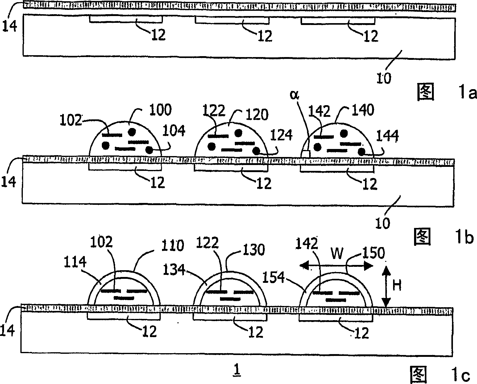
[0031] FIG. 1 a shows a carrier 10 including an optional electrode structure 12 . It should be emphasized that Figure 1 and the following figures show an embedded electrode structure 12 for reasons of clarity only. It should be understood that the surface of the carrier 10 is preferably also defined by the arrangement of the electrode structures 12 on top of the carrier 10 . The electrode structure 12 may be formed from a known material, such as indium tin oxide (ITO), on top of the carrier 10 by known techniques for forming electrode structures on the carrier 10 . The carrier 10 may comprise any suitable material, such as glass, polymers, or even non-obvious materials such as modified wood, ceramic or modified paper.

[0032] Optionally, the surfa...


PUM


Abstract

The electronic device ( 1 ) of the present invention has a carrier ( 10 ) with a plurality of discrete electro-optical elements ( 110, 130, 150 ) mounted on the surface of the carrier ( 10 ). The electro-optical elements ( 110, 130, 150 ), which cover respective parts of the electrode structure ( 12 ) on the surface of the carrier ( 10 ), each have a polymer layer ( 114, 134, 154 ), which encloses an electro-optical material ( 102, 122, 142 ) between the polymer layer ( 114, 134, 154 ) and the surface of the carrier ( 10 ). The discrete electro-optical elements ( 110, 130, 150 ) have been formed by the individual deposition of discrete droplets of a liquid comprising the electro-optical material and a polymer precursor followed by exposure of the droplets to a stimulus triggering the polymerization of the polymer precursor.

Description

technical field [0001] The invention relates to a method of manufacturing a display device comprising a plurality of discrete liquid crystal elements on the surface of a carrier. [0002] The invention also relates to a display device comprising a carrier comprising a plurality of cholesteric liquid crystal elements on the surface of the carrier. Background technique [0003] Now, many flat panel display devices use the photoelectric effect of liquid crystal materials to realize display functions. A special class of liquid crystal displays (LCDs) are cholesteric textured liquid crystal (CTLC) displays. An important property of CTLC displays is that they are infinitely multiplexable, ie the individual LC elements remain in their driven state. This is caused by the bistable nature of the cholesteric liquid crystal (CLC) material, which has the important advantage of low power consumption in the standby mode of the CTLC device since the state of the LC element does not have t...

Claims


Application Information

Patent Timeline
IPC IPC(8): G02F1/1334G02F1/137G02F1/1347G02F1/1333
CPCG02F1/133377G02F1/1334
Inventor J·P·A·福格尔斯D·J·布洛尔R·彭特尔曼S·I·克林克P·C·杜伊内维尔德
Owner KONINKLIJKE PHILIPS ELECTRONICS NV
Learn More