Surface conducting field emission electronic source device with convergent characteristic

A field emission, electron source technology, applied in the direction of cathode ray tube/electron beam tube, electrical components, discharge tube/lamp parts, etc., can solve problems such as electron beam divergence, achieve low driving voltage, simple process, high efficiency high effect

Inactive Publication Date: 2006-10-11
OCEAN UNIV OF CHINA
View PDF0 Cites 5 Cited by
  • Summary
  • Abstract
  • Description
  • Claims
  • Application Information

AI Technical Summary

Problems solved by technology

[0004] The basic concept of the present invention is to change the electrode structure of the conventional field emission electron source so that the electron-emitting cathode surrounds the grid, so that the electrons emitted from the cathode converge to the grid, so as to solve the problem of the conventional surface conduction type (SED type) and micro Problems of Electron Beam Divergence in Pointed Field Emission Electron Source

Method used


Image

  • Surface conducting field emission electronic source device with convergent characteristic
  • Surface conducting field emission electronic source device with convergent characteristic
  • Surface conducting field emission electronic source device with convergent characteristic

Examples


Embodiment Construction

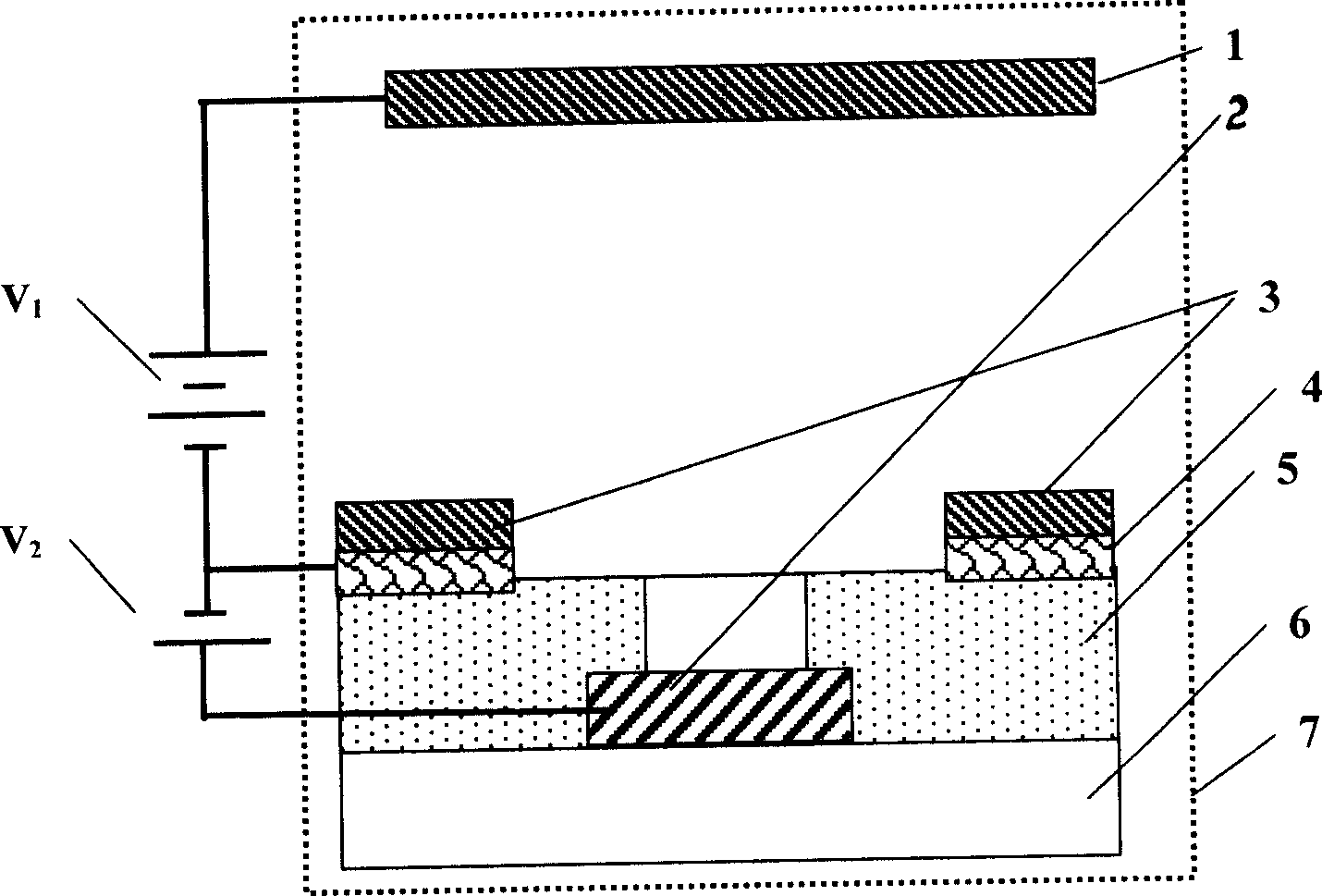
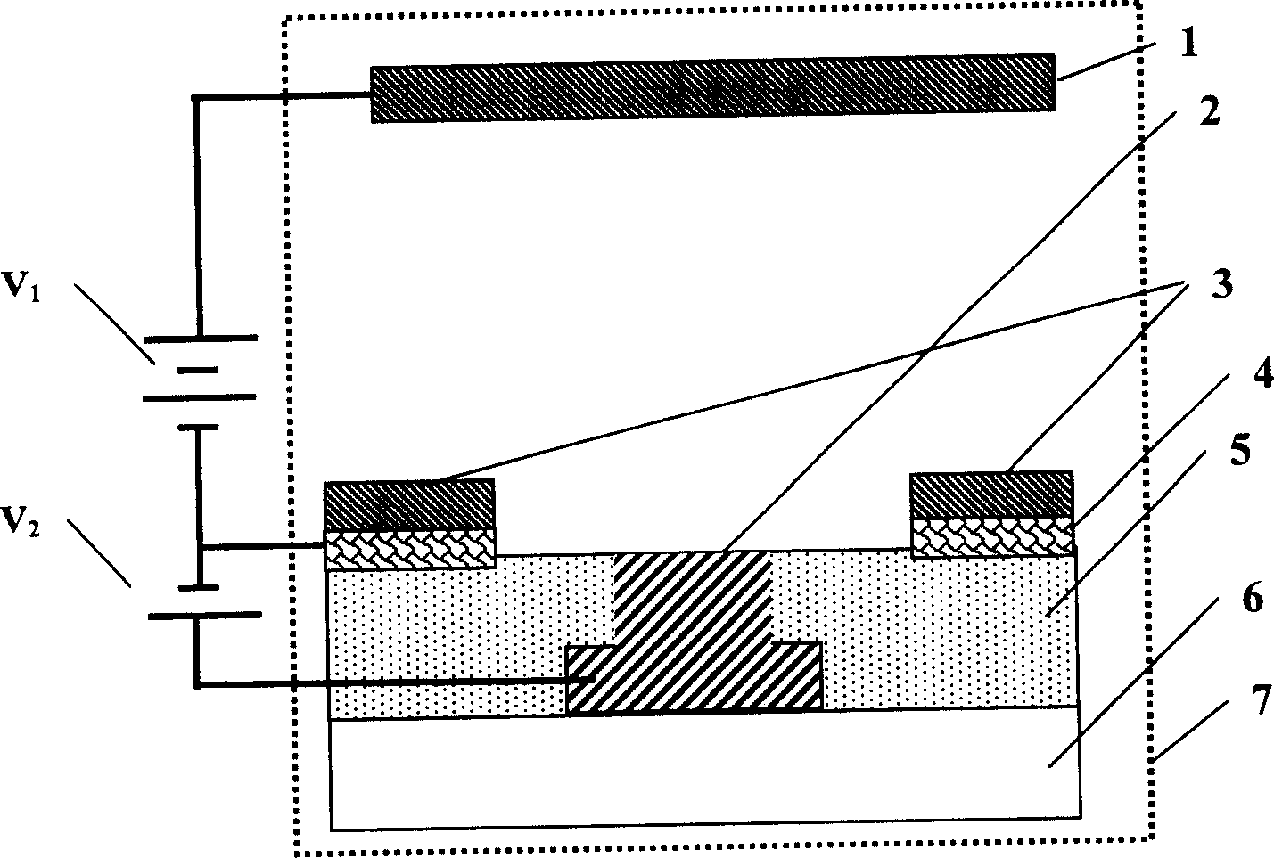
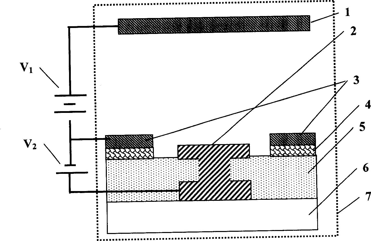
[0022] Such as figure 1 , the present invention includes the grid 2 on the substrate 6, the cathode 3 and the insulating layer 5, and the anode 1 with a certain distance opposite to it, and is contained and fixed in the vacuum cavity 7 and a suitable power supply, and is characterized in that the grid The electrode 2 is located between the insulating layer 5 and the substrate 6 , and the grid 2 exposed from the insulating layer 5 through the hole is surrounded by the cathode 3 , and an electron emission layer 4 is arranged between the cathode 3 and the insulating layer 5 .

[0023] Electron emission layer 4 can be the particle material such as metal, metal oxide, semiconductor, particle size is less than 50 microns, or by the mixture of above materials; Low-dimensional materials mainly include one-dimensional, quasi-one-dimensional, two-dimensional, quasi-two-dimensional nano-metals, metal oxides, elements or compound semiconductor materials. The function of the electron emis...


PUM


Abstract

The disclosed surface-conductive field-emission electron source device with convergence feature comprises a substrate with an inverted-T shaped or I-shaped grid, a cathode and an insulating layer, and an opposite anode fixed in a vacuum cavity. Wherein, arranging the grid between the insulating layer and the substrate, showing the grid through a hole to circle by the cathode; arranging an electron emission layer between the cathode and the insulating layer, and adding a layer of cathode between the emission layer and the insulating layer to form a sandwich cathode, as well as an electron scattering layer between the cathode and shown grid. This invention needs simple technique and low drive voltage, and has well electron convergence performance.

Description

technical field [0001] The invention relates to a device for obtaining electron beams in a vacuum environment by using the field electron emission (referred to as field emission) phenomenon---a surface conduction field emission electron source device with convergence characteristics Background technique [0002] The usual field emission electron source device uses electrons (field emission phenomenon) that escape from the surface of solid materials under the action of a strong external electric field, and uses the electric field applied by the gate and anode to realize the emission, modulation and acceleration of electrons to obtain luminescence, high Electronic devices with functions such as frequency oscillation and X-rays. At present, there are many kinds of field emission electron source device structures, such as metal or semiconductor microtip + circular hole gate (referred to as microtip type), surface conduction type (SED type), metal-insulator layer-metal (referred ...

Claims


Application Information

Patent Timeline
Patent Type & Authority Applications(China)
IPC IPC(8): H01J29/02H01J29/04H01J1/304H01J1/46H01J31/12
Inventor 元光蒋进京
Owner OCEAN UNIV OF CHINA
Why Eureka
Try Eureka