

Organic el device and display
An organic and organic layer technology, applied in electroluminescence light source, electric solid state device, electric light source, etc., can solve the problems of insufficient balance of luminous intensity, display application, insufficient half-life of luminous efficiency and brightness, etc. Excellent color reproduction performance, high efficiency and long-term stability
- Summary
- Abstract
- Description
- Claims
- Application Information
AI Technical Summary
Problems solved by technology
Method used
Image

Examples
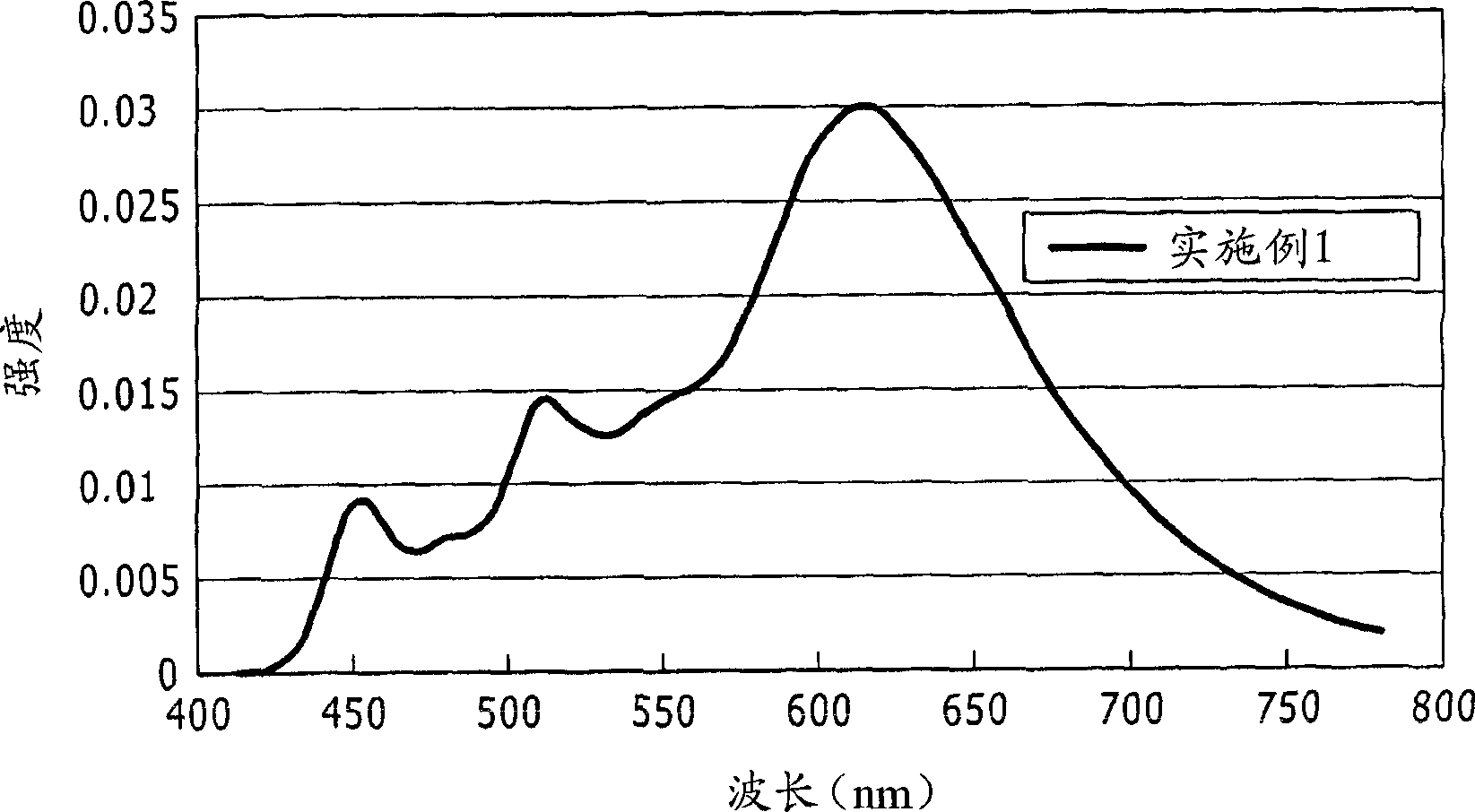
Embodiment 1
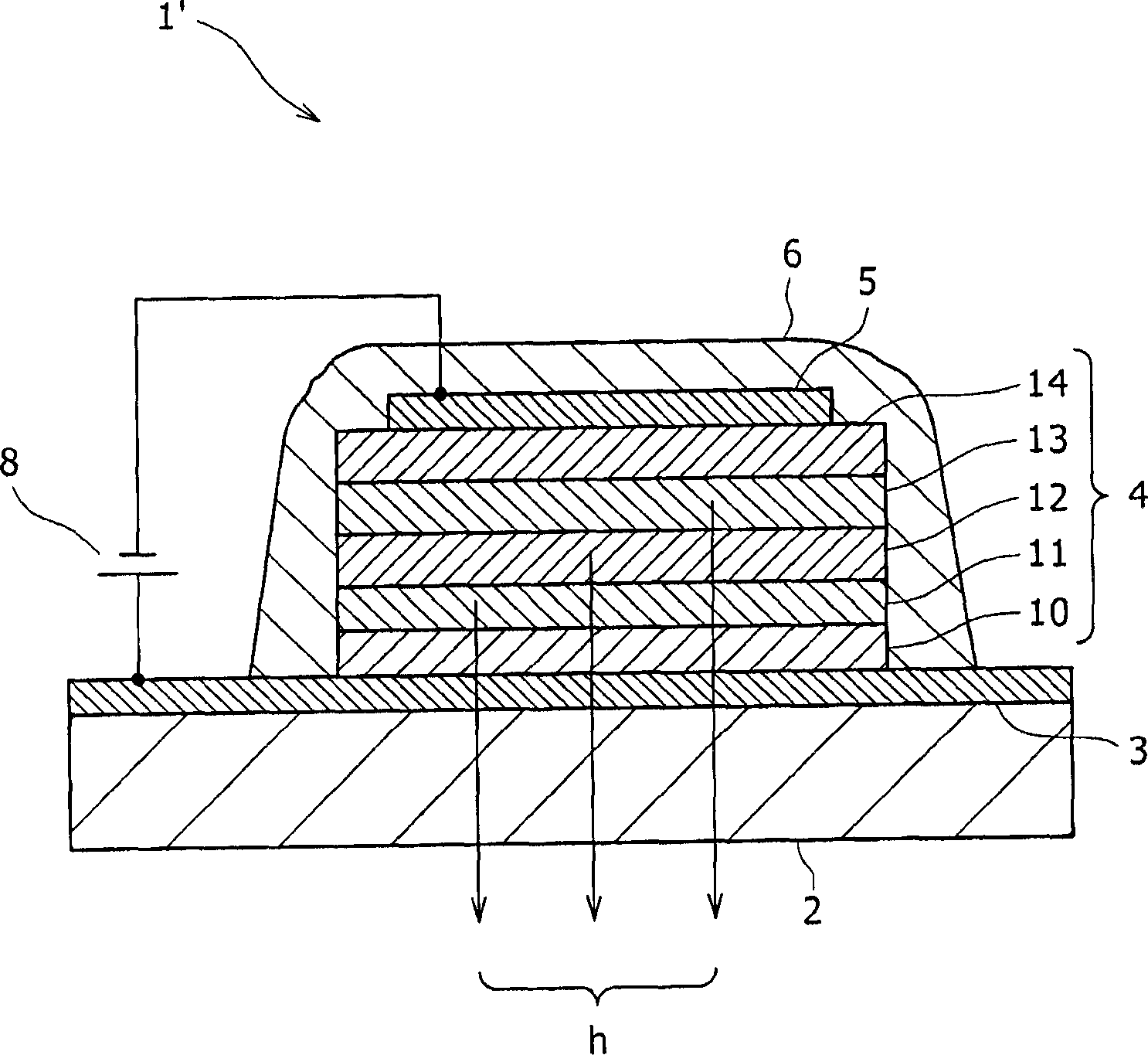
[0070] In Example 1, reference was made as follows figure 2 Bottom-emitting organic EL device 1' is described.
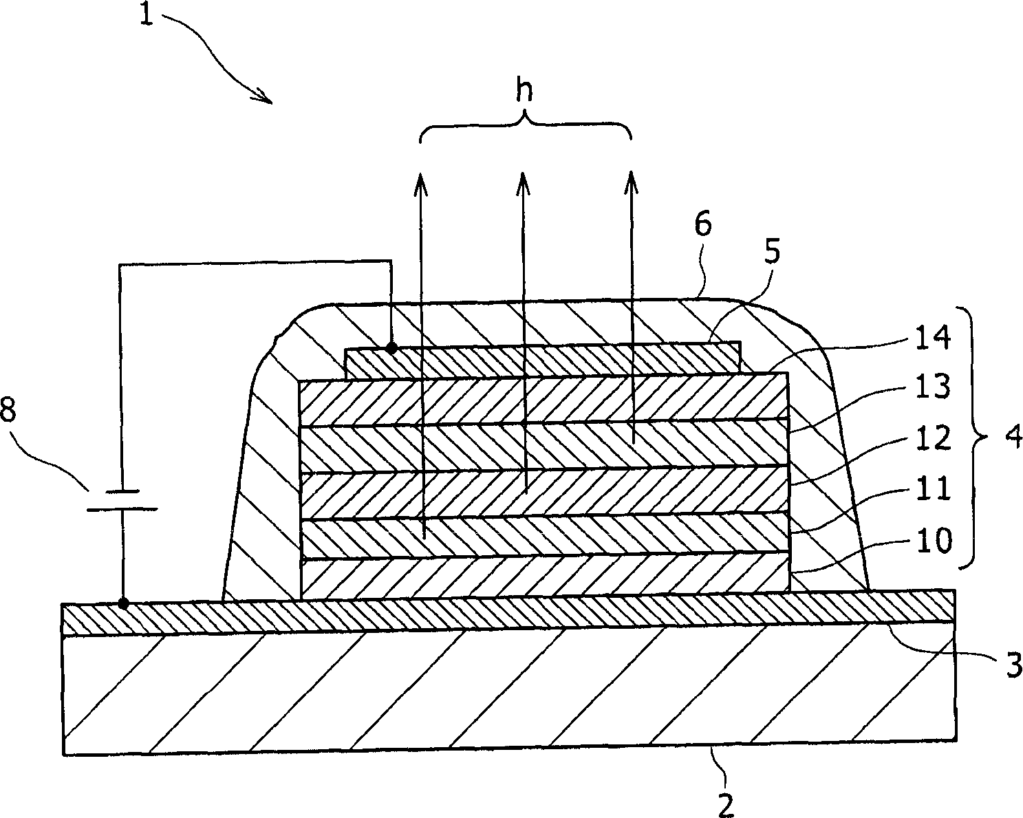
[0071] First, a unit for an organic EL device is produced in which an ITO film (approximately 100 nm thick) as an anode 3 is formed on a substrate 2 composed of a glass plate of 30 mm × 30 mm, and the anode 3 except for the central 2 mm × 2 mm light Other areas than the emission area are masked with an insulating film (omitted in the figure) by using a photosensitive organic insulating material. Next, under the condition that the opening matches the exposed portion of the anode 3 (ITO) that will become each light-emitting region, a metal mask with an opening is configured on the upper side of the substrate 2 and close to the substrate 2, and at 10 -4 The following organic layers were sequentially formed by a vacuum evaporation method at a vacuum of Pa or lower.
[0072] First, as the hole transport layer 10, a film of m-MTDATA (4,4',4"-tris(3-methylphenylanilino)...
Embodiment 2
[0091] In Example 2, the organic EL device 1' was fabricated in the same manner as above, except that the blue light emitting layer 13 of Example 1 used a two-layer structure of a positive and negative charge transporting blue light emitting layer and an electron transporting light emitting layer as described below other than to obtain a well-balanced white light emission.
[0092] In Example 2, an organic EL device 1' was manufactured by the same procedure as in Example 1, except that the blue light emitting layer 13 was formed by the following procedure. First, a co-deposited film consisting of a mixture of DPVBi and α-NPD at a mixing ratio of 1:1 doped with 3% of BCzVBi as a blue light-emitting material as a host was formed to a thickness of 10 nm. Then, a co-deposited layer consisting of DPVBi doped with 3% of BCzVBi as a blue light emitting material as a host doped with a thickness of 20 nm was formed to obtain a blue light emitting layer 13 having a laminated structure. ...
PUM
| Property | Measurement | Unit |
|---|---|---|
| luminance | aaaaa | aaaaa |
Abstract
Description
Claims
Application Information