

Plasma etching device exhaustring
A plasma and etching device technology, which is applied in the manufacturing of plasma, electrical components, semiconductor/solid-state devices, etc., can solve the problems of affecting the process window, reducing the gas conduction efficiency, etc., and achieve the effect of increasing the grounding area
- Summary
- Abstract
- Description
- Claims
- Application Information
AI Technical Summary
Problems solved by technology
Method used
Image

Examples
Embodiment 1
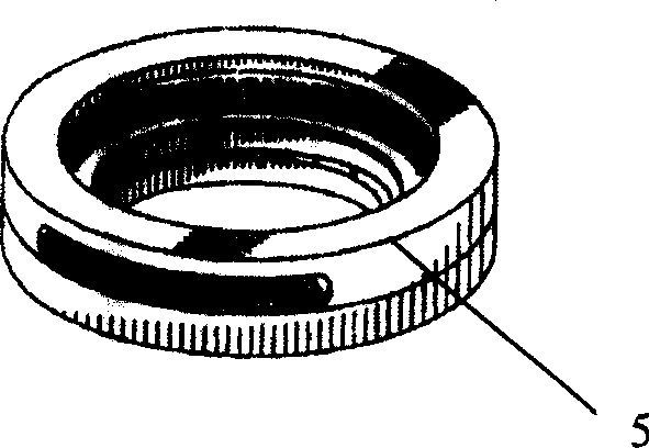
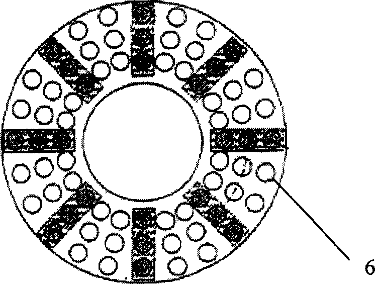
[0035] The exhaust ring structure of this embodiment is as follows Figure 7 , 8 shown. in, Figure 7 is a top view of the exhaust ring of the present embodiment, Figure 8 It is a vertical section along the A-A line. The upper part of the funnel-shaped hole is cone-shaped, and its cone angle is in the range of 10° to 45°, which is 3° in this embodiment. The lower part of the funnel-shaped hole is cylindrical, and the inner diameter of the cylinder should be smaller than the thickness of the plasma sheath, which is usually about 1-2mm. On the upper surface of the exhaust ring, that is, on the side surface 15 in contact with the plasma, there is an insulating coating sprayed Y 2 o 3 The material has a thickness of 50-150 μm, which is 100 μm in this embodiment. due to Y 2 o 3 The corrosion resistance is high, therefore, during the implementation of the etching process, damage can be reduced, pollution can be reduced, and the yield rate can be improved.
[0036] The exh...
Embodiment 2
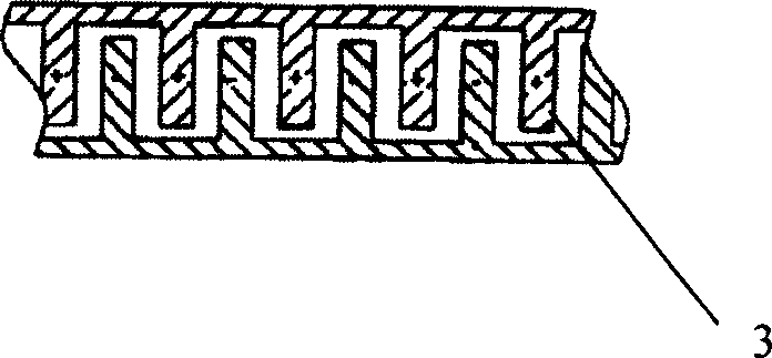
[0038] The exhaust ring structure of this embodiment is as follows Figure 9 shown. in, Figure 9 It is a perspective view of the exhaust ring of this embodiment. It can be seen that the holes on the exhaust ring are elongated. The upper taper angle of the funnel-shaped hole of the hole is 40°. On the plasma space side surface of the exhaust ring, there is an insulating coating sprayed with Al 2 o 3 material with a thickness of 150 μm. Thanks Al 2 o 3 The corrosion resistance is high, therefore, during the implementation of the etching process, damage can be reduced, pollution can be reduced, and the yield rate can be improved.
[0039] According to the present invention, by adopting the funnel-shaped exhaust ring structure, plasma leakage can be suppressed, the grounding area can be increased, and abnormal plasma discharge can be suppressed. 2 o 3 or Al 2 o 3 Spraying can reduce exhaust ring damage, reduce metal particle pollution, and improve yield.
Embodiment 3
[0041] The exhaust ring structure of this embodiment is as follows Figure 9 As shown, the holes on the exhaust ring are elongated. In this embodiment, the upper taper angle of the funnel-shaped hole of the hole is 5.5°. On the surface of the plasma space side of the exhaust ring, there is an insulating coating sprayed Y 2 o 3 material with a thickness of 50 μm. due to Y 2 o 3 The corrosion resistance is high, therefore, during the implementation of the etching process, damage can be reduced, pollution can be reduced, and the yield rate can be improved.
[0042] According to the present invention, by adopting the funnel-shaped exhaust ring structure, plasma leakage can be suppressed, the grounding area can be increased, and abnormal plasma discharge can be suppressed. 2 o 3 or Al 2 o 3 Spraying can reduce exhaust ring damage, reduce metal particle pollution, and improve yield.
PUM
| Property | Measurement | Unit |
|---|---|---|
| Thickness | aaaaa | aaaaa |
Abstract
Description
Claims
Application Information