Manufacture by Dimashg process

A manufacturing method and process technology, which is applied in the field of Damascus process to manufacture integrated circuits, can solve problems such as failure, cumbersome process, and complicated subsequent etching process, and achieve the effect of shortening etching and improving the pass rate

Inactive Publication Date: 2006-11-01
SHANGHAI INTEGRATED CIRCUIT RES & DEV CENT +1
View PDF0 Cites 4 Cited by
  • Summary
  • Abstract
  • Description
  • Claims
  • Application Information

AI Technical Summary

Problems solved by technology

Full via first method (Full VIA First) This process has no alignment problem, no via failure problem and a large process window, but the problem is mainly concentrated in the via filling step, failed via filling or uneven filling The performance will inevitably lead to adverse reactions in the subsequent process, or even failure, and the conventional filling reagent and subsequent photolithography process use a variety of different types of chemical substances, the process is cumbersome, and the subsequent etching process is complicated

Method used


Image

  • Manufacture by Dimashg process
  • Manufacture by Dimashg process
  • Manufacture by Dimashg process

Examples


Embodiment Construction

[0031] Now in conjunction with accompanying drawing, the specific embodiment of the present invention is described in further detail:

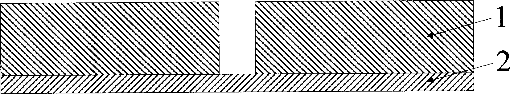
[0032] Firstly, a through-hole dielectric layer 1 at the bottom layer of damascene is deposited.

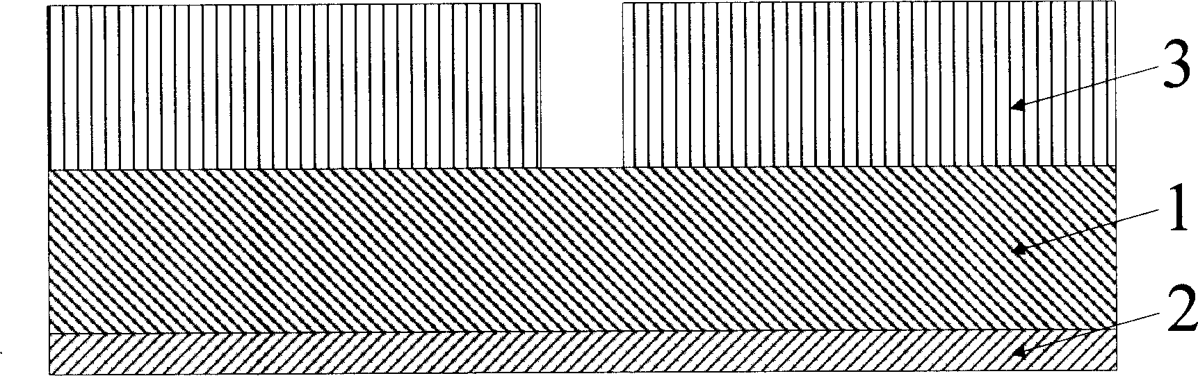
[0033] Secondly, if Figure 3A as shown ( Figure 3A For the schematic diagram of coating the first single-layer photosensitive material), the first layer of single-layer photosensitive material 3 is coated on the surface of the through-hole dielectric layer of the damascene bottom layer, and photolithography is performed. The first single-layer photosensitive material is composed of ketones, ethers, alkane organic solvents and photosensitive cross-linking resins, and the molecular weight is between 85,000 and 150,000.

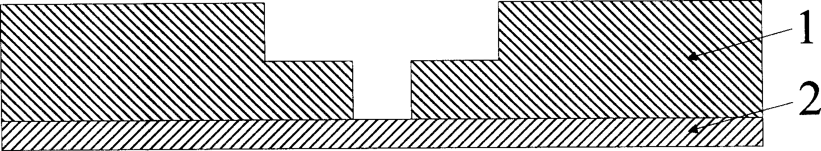
[0034] Secondly, if Figure 3B as shown ( Figure 3B is a schematic diagram of through-hole etching), and through-hole etching and cleaning are performed on the through-hole dielectric layer at the bottom of the damascene. T...


PUM


Abstract

The method uses the intercombination of double layer light sensitiveness material and single layer light sensitiveness material, and employs multiple steps process to manufacture through-hole and metal wire slot, and uses Damascus Process to make integrated circuit. The Damascus Process is a new wiring technology having problem of filling through hole. The invention uses a new process that is: first completing the filling of through hole; then after plasma processing, using the double layer light sensitiveness material to form an oxidizing coating to overlap the through hole; and later, making deposition and fabricating metal wire slot so as to achieve fabrication process.

Description

technical field [0001] The invention belongs to the technical field of integrated circuit technology, and in particular relates to a method for manufacturing integrated circuits by using a Damascus process in which double-layer photosensitive materials and single-layer photosensitive materials are combined with each other. Background technique [0002] With the continuous improvement of integrated circuit manufacturing technology, the volume of semiconductor devices is becoming smaller and smaller, and it is more difficult to connect them. In the past 30 years, the semiconductor industry has used aluminum as the material for connecting devices, but as chips shrink, the industry needs thinner and thinner connections, and the high resistance of aluminum is becoming more and more difficult to meet. need. Moreover, in the case of high-density VLSI, high resistance can easily cause electrons to "jump wires", causing nearby devices to produce false switching states. That is to s...

Claims


Application Information

Patent Timeline
Patent Type & Authority Applications(China)
IPC IPC(8): H01L21/768G03F7/004H01L21/3205
Inventor 朱骏
Owner SHANGHAI INTEGRATED CIRCUIT RES & DEV CENT
Why Eureka
Try Eureka