
Plasma processing apparatus and method

A plasma and processing device technology, applied in the field of plasma processing devices, can solve the problems of high manufacturing cost, hindering uniform electromagnetic field, uneven plasma, etc.

Inactive Publication Date: 2006-11-01
TOKYO ELECTRON LTD +1
View PDF2 Cites 11 Cited by
  • Summary
  • Abstract
  • Description
  • Claims
  • Application Information

AI Technical Summary

Problems solved by technology

[0003] However, as the size of the substrate increases, the processing equipment also becomes larger. In particular, it is difficult to manufacture a large-sized dielectric body, and the manufacturing cost is high.
In addition, when the dielectric body is large and heavy, the supporting member supporting it must have a strong structure, but thus, the problem of unevenness of the plasma generated in the processing chamber is likely to occur.
That is, the enlarged support member becomes an obstacle, preventing the formation of a uniform electromagnetic field over the entire substrate
In addition, due to the large area of ​​the dielectric itself, it is difficult to uniformly propagate microwaves over the entire surface of the dielectric due to various conditions such as the type of processing gas or the pressure in the processing chamber.

Method used


Image

  • Plasma processing apparatus and method
  • Plasma processing apparatus and method
  • Plasma processing apparatus and method

Examples


Embodiment Construction

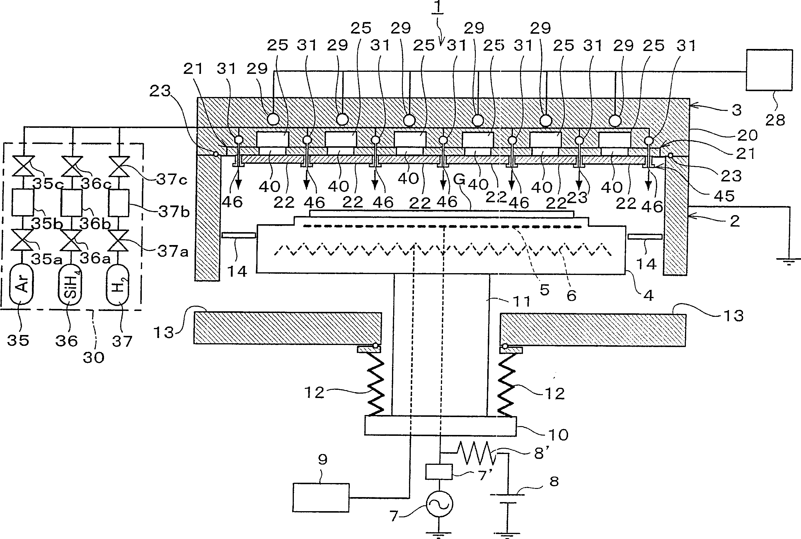
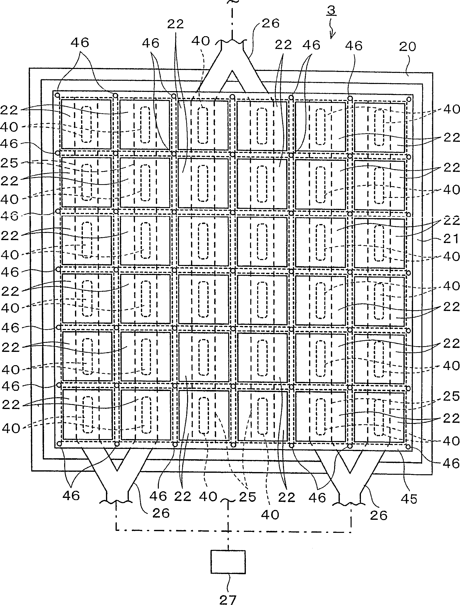
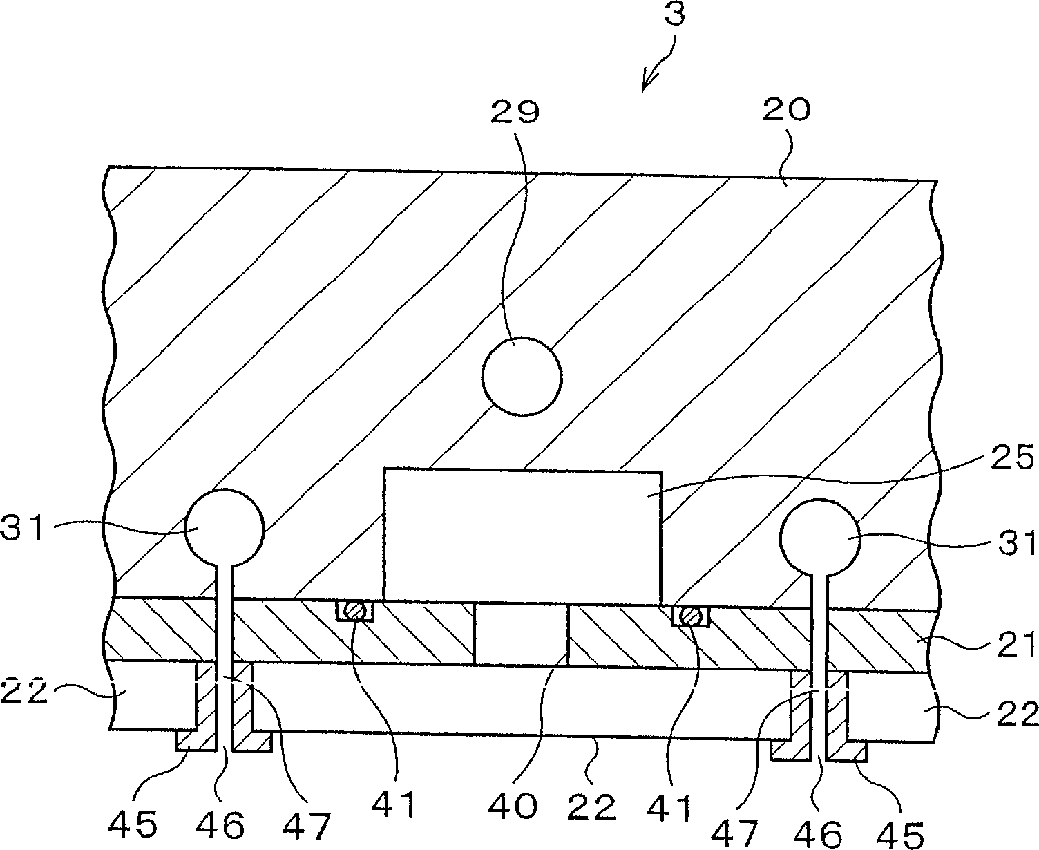
[0019] Hereinafter, an embodiment of the present invention will be described based on a plasma processing apparatus 1 that performs CVD (Chemical Vapor Deposition) processing as an example of plasma processing. figure 1 It is a vertical cross-sectional view showing a schematic configuration of the plasma processing apparatus 1 according to the embodiment of the present invention. figure 2 It is a bottom view showing the arrangement of a plurality of dielectric bodies 22 supported on the lower surface of the lid body 3 included in the plasma processing apparatus 1 . image 3 It is a partially enlarged longitudinal sectional view of the cover body 3 .

[0020] The plasma processing apparatus 1 includes a bottomed cuboid processing container 2 with an open top, and a cover 3 that closes the processing container 2 . The processing container 2 and the cover body 3 are made of aluminum, and both are grounded.

[0021] A susceptor 4 is provided inside the processing container 2 an...


PUM


Abstract

A plasma processing apparatus that passes a microwave, which is introduced into a waveguide, through a slot and propagates the microwave to a dielectric, converts a predetermined gas supplied into a processing chamber into plasma, and applies plasma processing to a substrate, in which a plurality of the waveguides are disposed side by side, a plurality of dielectrics are provided for each of the waveguides, and one slot, or two or more slots is or are provided for each of the dielectrics, is provided. The area of each of the dielectrics can be made extremely small, and a microwave can be reliably propagated into the entire surface of the dielectric. A thin support member that supports the dielectric can be used, a uniform electromagnetic field can be formed in an entire area above the substrate, and uniform plasma can be generated in the processing chamber.

Description

technical field [0001] The present invention relates to a plasma processing apparatus and method for generating plasma and performing processing such as film formation on a substrate. Background technique [0002] For example, in the manufacturing process of LCD devices and the like, microwaves are used to generate plasma in a processing chamber to perform CVD processing, etching processing, etc. on an LCD substrate. As a plasma processing apparatus, a device in which a plurality of waveguides are arranged in parallel above a processing chamber is known (see JP-A-2004-200646 and JP-A-2004-152876). A plurality of grooves are arranged in parallel on the lower surface of the waveguide, and a flat dielectric body is provided along the lower surface of the waveguide. The equipment is configured such that microwaves are propagated to the surface of the dielectric body through the grooves, and the processing gas (rare gas for plasma excitation and / or gas for plasma processing) sup...

Claims


Application Information

Patent Timeline
Patent Type & Authority Applications(China)
IPC IPC(8): H05H1/46H01J37/32H01L21/00
Inventor 北村昌幸平山昌树大见忠弘
Owner TOKYO ELECTRON LTD
Learn More