
Apparatus and method for verificating chip standard coincidence degree

A verification method and verification equipment technology, which is applied in the field of chip standard compliance verification equipment, can solve problems such as error-prone, high manpower input costs, and normal failure to be guaranteed, and achieve high input and output effects

Inactive Publication Date: 2006-11-15
HUAWEI TECH CO LTD
View PDF0 Cites 4 Cited by
  • Summary
  • Abstract
  • Description
  • Claims
  • Application Information

AI Technical Summary

Problems solved by technology

[0007] A. It is very time-consuming to change the working mode of the central office chip and terminal chip after each parameter test is completed, and it may be necessary to modify the configuration of multiple parameters of the central office chip and terminal chip every time the working mode is adjusted, which is prone to errors and improves efficiency. too low
[0008] B. Because there are too many parameters defined in the standard, it is impossible to traverse every combination of parameters by manual testing, and only the most commonly used combinations can be used for verification. In this way, it cannot be guaranteed whether the functions of those combinations that are not commonly used are normal. There may be problems in the environment
[0009] C. Because the local end chip and terminal chip version technology is immature, and the manufacturers have insufficient experience, each upgrade may cause a new problem of another parameter while solving the old problem of one parameter. In order to ensure the correctness of all functions, it is necessary to All parameters are fully verified, so the cost of manpower input for each upgrade is too high

Method used


Image

  • Apparatus and method for verificating chip standard coincidence degree
  • Apparatus and method for verificating chip standard coincidence degree

Examples


Embodiment Construction

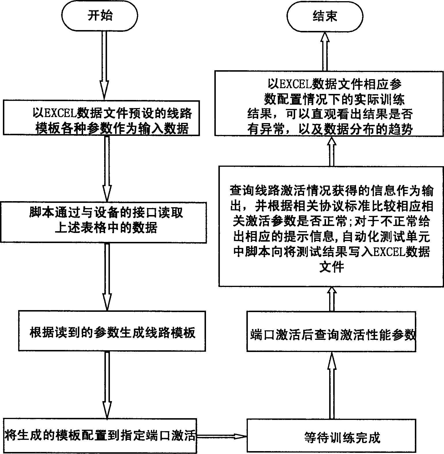
[0034] A chip standard compliance verification device and method of the present invention will be further described in detail below in conjunction with the accompanying drawings.

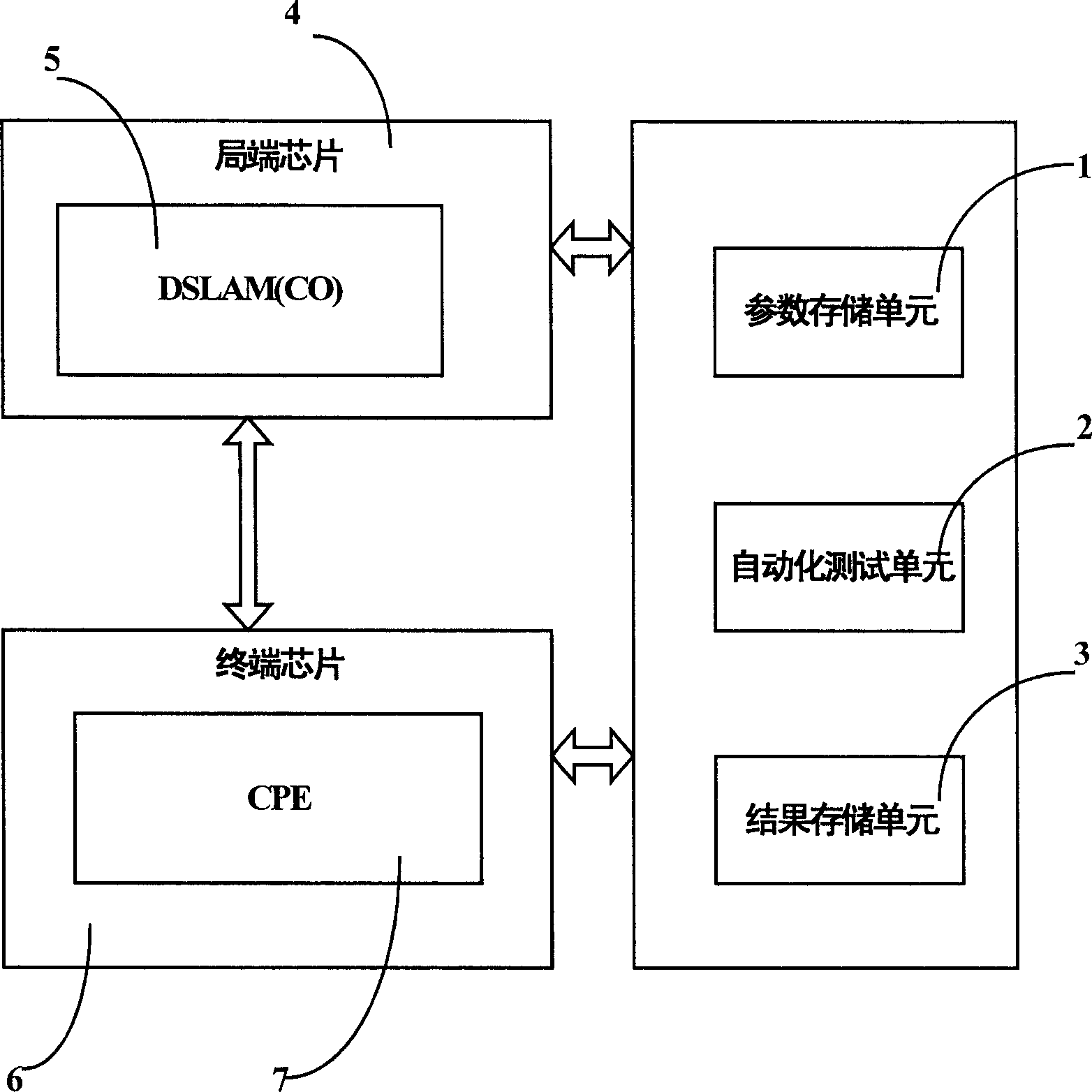
[0035] A kind of chip standard conformity verification equipment and method of the present embodiment is particularly described with ADSL2+, ADSL chip standard conformity verification equipment and method, but the present invention is equally applicable except the chip standard mentioned above The case of communicating with any other communication chip standards.

[0036] The chip standard seat verification device of the present invention includes a parameter storage unit 1 , an automatic test unit 2 and a result storage unit 3 .

[0037] The parameter storage unit 1 is used to store various parameters of the line template, including the hardware configuration environment and software configuration environment parameters required for functional verification, and for the functional verification of di...


PUM


Abstract

The invention is a chip standard conformity verifying device and method, comprising: automated testing unit, for reading chip parameter data and packing and transmitting them to the chip, reading various performance parameters of activated chip ports, reconstructing data and analyzing various activation parameters; parameter storage unit, for storing various chip performance parameters; result storage unit, for storing port performance parameters and analyzed results of the automated testing unit. And it implements related standard conformity verification on cooperating functions of branch chips and terminal chips of different manufactures, having completely high yield.

Description

technical field [0001] The invention relates to the field of communication detection, in particular to a chip standard compliance verification device and method. Background technique [0002] The asymmetrical digital subscriber loop (Asymmetrical Digital Subscriber Loop, ADSL) technology is based on ordinary telephone lines to provide terminal customers with a last-mile broadband access means. Since 2000, ADSL technology has stood out among several broadband access technologies, and has become a market-leading access method due to its excellent cost performance, and has gradually evolved along the path of ADSL→ADSL2→ADSL2+, with continuously increasing bandwidth, continuously enhancing functions, and stable The sex keeps improving. [0003] All digital subscriber line access multiplexer (Digital Subscriber Line Access Multiplexer, DSLAM) equipment supporting ADSL, ADSL2, ADSL2+ services must follow certain international standards in order to realize the interoperability bet...

Claims


Application Information

Patent Timeline
IPC IPC(8): H04M3/30
Inventor 王吉辉
Owner HUAWEI TECH CO LTD
Learn More