Display device, manufacturing method thereof, organic light emitting device, and manufacturing method thereof

一种有机发光装置、显示装置的技术,应用在有机发光装置及其制造,表面发光型显示装置领域,能够解决降低发光效率、差色泽复现性显示装置、电能消耗和器件寿命大负担等问题

Active Publication Date: 2006-11-22
SONY CORP
View PDF4 Cites 75 Cited by
  • Summary
  • Abstract
  • Description
  • Claims
  • Application Information

AI Technical Summary

Problems solved by technology

However, in configuration (2), the color filter absorbs unnecessary luminescent components, thereby reducing luminous efficiency, resulting in a large burden on power consumption and device lifetime
In addition, it is difficult to filter the white light emitted by the light-emitting device into blue, green, and red colors with favorable color purity through the transmission characteristics of the color filter that can be mass-produced, only to produce the extracted light with a wide wavelength distribution and poor Display device with color reproducibility
In addition, in the configuration (3), there are problems such as low conversion efficiency of the color conversion filter, difficulty in manufacturing the color conversion filter, lifetime of the color conversion filter, color purity of the luminescent color after color conversion, and so it is difficult to convert the color conversion filter put the above structure into practical use

Method used


Image

  • Display device, manufacturing method thereof, organic light emitting device, and manufacturing method thereof
  • Display device, manufacturing method thereof, organic light emitting device, and manufacturing method thereof
  • Display device, manufacturing method thereof, organic light emitting device, and manufacturing method thereof

Examples


no. 1 example

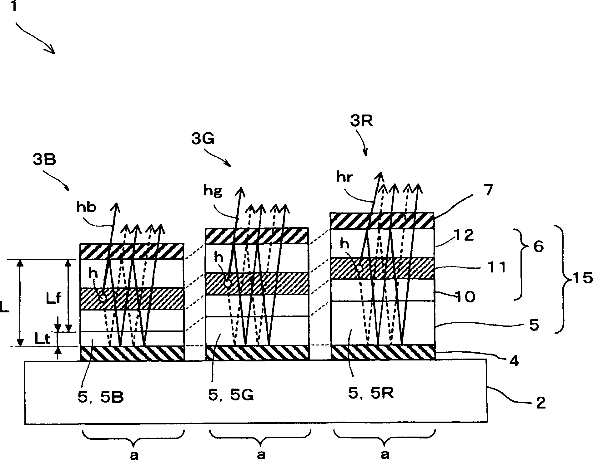
[0059] First, refer to figure 1 A display device according to a first embodiment of the present invention will be described. figure 1 is a cross-sectional view of a model illustrating a configuration example of a display device according to this embodiment. The display device 1 in the illustration is a full-color display device in which each organic EL device 3B, 3G, and 3R is arranged and formed on a substrate 2, each of blue (B), green (G), and red (R) Colors emanate from it. The display device 1 displays images using the organic EL phenomenon. Each of the organic EL devices 3B, 3G, and 3R has a configuration in which a lower electrode 4 , a transparent conductive layer 5 , a functional layer 6 , and an upper electrode 7 are layered from the substrate 2 side. The display device is configured as a top emission type display device in which emitted light h emitted in the functional layer 6 is extracted from the side of the upper electrode 7 opposite to the substrate 2 . The...

no. 2 example

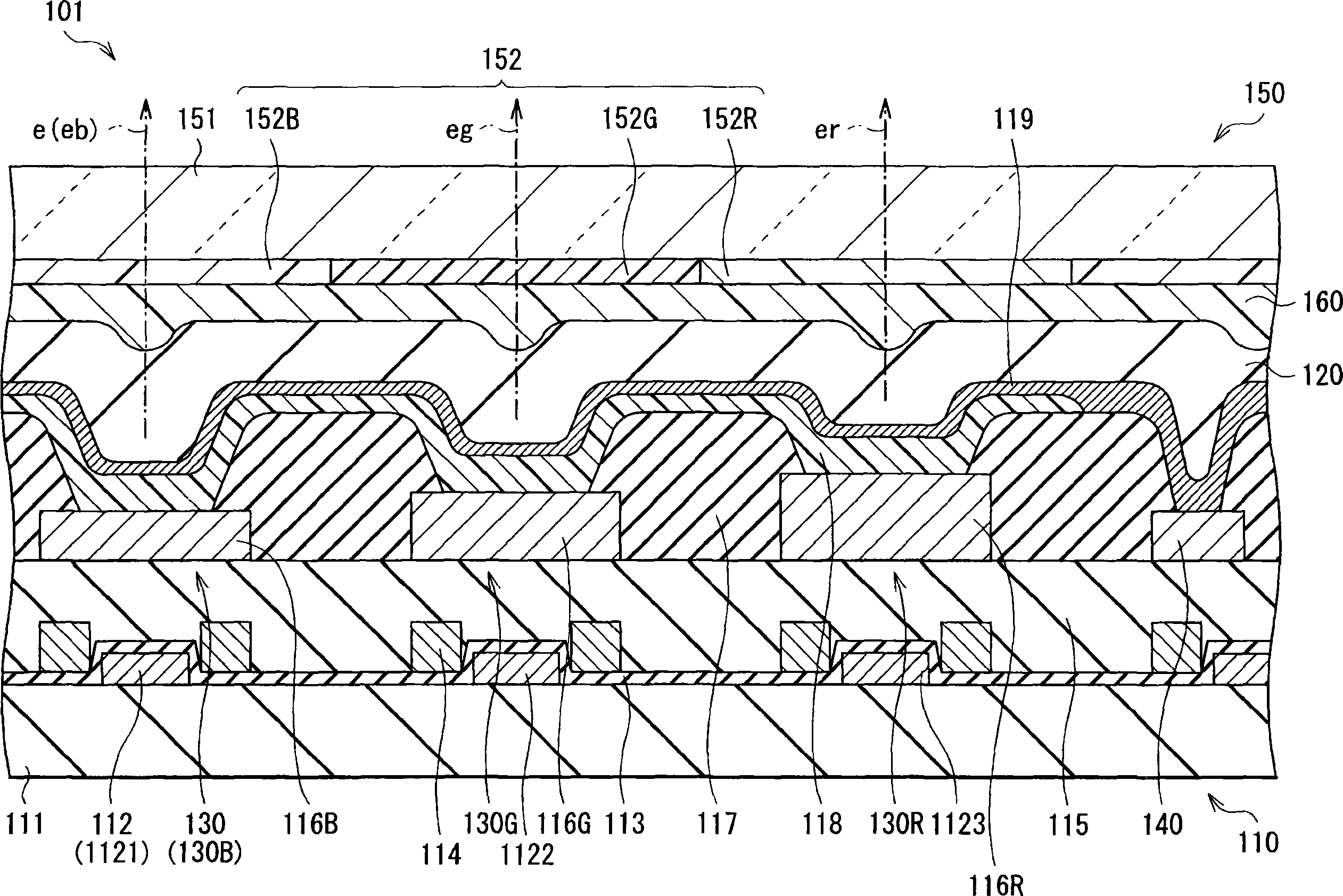
[0102] Next, we will refer to image 3 A display device according to a second embodiment of the present invention will be described. image 3 A cross-sectional configuration of the display device 101 is shown.

[0103] The display device 101 displays images using the organic EL phenomenon. For example, if image 3 As shown, in the case where the organic light-emitting device is equipped with an organic EL device 130 and a driving device (TFT: Thin Film Transistor) 112 for driving the organic EL device 130, the driving panel 110 and the sealing panel 150 are relatively arranged, and the intermediate The adhesive layer 160 bonds the driving panel 110 and the sealing panel 150 together, thereby sandwiching the organic EL device 130 between the driving panel 110 and the sealing panel 150 . For example, the display device 101 has a top emission type structure for emitting light e generated in the organic EL device 130 upward, that is, toward the outside of the sealing panel 150 ...

no. 3 example

[0175] Next, a third embodiment of the present invention will be described.

[0176] The display device according to this embodiment has a structure similar to that of the display 101 described in the second embodiment above ( Figure 3 to Figure 5 ) structure, except that the formation steps of the lower electrode layers 116R, 116G, and 116B are different, the display device according to this embodiment can be manufactured using manufacturing steps similar to those of the display 101 . In this embodiment, specifically, for example, in order to accurately form the barrier layers 1163R, 1163G, and 1163B of the lower electrode layers 116R, 116G, and 116B, the barrier layer portion 11631 is preferably made of tin oxide (SnO 2 ) or chromium oxide (CrO), the barrier layer portion 11632 is composed of ITO, and the barrier layer portion 11633 is composed of IZO.

[0177] Figure 12 to Figure 19 The role of is to explain the manufacturing steps of the lower electrode layers 116R, 11...


PUM


Abstract

There are provided a display device capable of simplifying design / manufacturing with a simplified light emitting element configuration while performing a highly accurate display with an excellent color reproduction, and a manufacturing method thereof. A function layer (6) including a light emitting layer (11) is sandwiched between a lower electrode (4) composed of a light reflection material and a light-translucent upper electrode (7). The light h emitted by the light emitting layer (6) is made to resonate between the lower electrode (4) and the upper electrode (7) as a resonance unit (15) and the light is taken out from the side of the upper electrode (7). A plurality of organic EL elements (3B, 3G, 3R) having such a resonator structure are arranged on a substrate (2) so as to constitute a display device (1). Each of the organic EL elements (3B, 3G, 3R) has the function layer (6) composed of the same layer and the resonator unit (15) has an optical distance L which is set to a different value so as to resonate the wavelength regions of blue, green, or red.

Description

technical field [0001] The present invention relates to a display device and a manufacturing method thereof, as well as an organic light-emitting device and a manufacturing method thereof. Specifically, the present invention relates to a surface emission type display device in which a light emitting device such as an organic EL device is arranged and formed on a substrate, and a desired luminous color can be selectively extracted (extracted), and furthermore, the present invention relates to said A method for manufacturing a surface-emitting display device, and an organic light-emitting device and a method for manufacturing the same. Background technique [0002] In recent years, as display devices have replaced cathode ray tubes (CRTs), research and development of flat panel displays that are light in weight, small in size, and low in power consumption have been active. As described above, display devices using organic light-emitting devices, including self-luminous displa...

Claims


Application Information

Patent Timeline
Patent Type & Authority Applications(China)
IPC IPC(8): H05B33/24H01L27/32H01L51/52H05B33/10H05B33/12H05B33/14
CPCH10K59/30H10K59/35H10K50/818H10K50/828H10K50/852H10K2102/3026H10K2102/351H10K59/805H01L27/153H10K50/805H10K59/38H10K50/81H10K50/82H10K50/813H10K50/824H10K50/841H10K50/856H10K59/124H10K59/131H10K59/1315
Inventor 柏原充宏山田二郎横山诚一花轮幸治
Owner SONY CORP
Why Eureka
Try Eureka