Electron emitting element, electron emitting device, display and light source

A technology of electron injection and components, applied in the field of light sources, can solve the problems of high manufacturing cost and complicated panel manufacturing process, and achieve the effects of reducing product cost, improving straightness, and realizing cost

Inactive Publication Date: 2006-11-29
NGK INSULATORS LTD
View PDF4 Cites 2 Cited by
  • Summary
  • Abstract
  • Description
  • Claims
  • Application Information

AI Technical Summary

Problems solved by technology

[0003] Conventional examples of such electron-emitting elements include Patent Documents 1 to 5, but since they do not use a dielectric in the emitter portion, molding or micro-fabrication is required between opposing electrodes, and it is necessary to apply High voltage, in addition, there is such a problem that the panel manufacturing process is complicated and the manufacturing cost is high

Method used


Image

  • Electron emitting element, electron emitting device, display and light source
  • Electron emitting element, electron emitting device, display and light source
  • Electron emitting element, electron emitting device, display and light source

Examples


Embodiment Construction

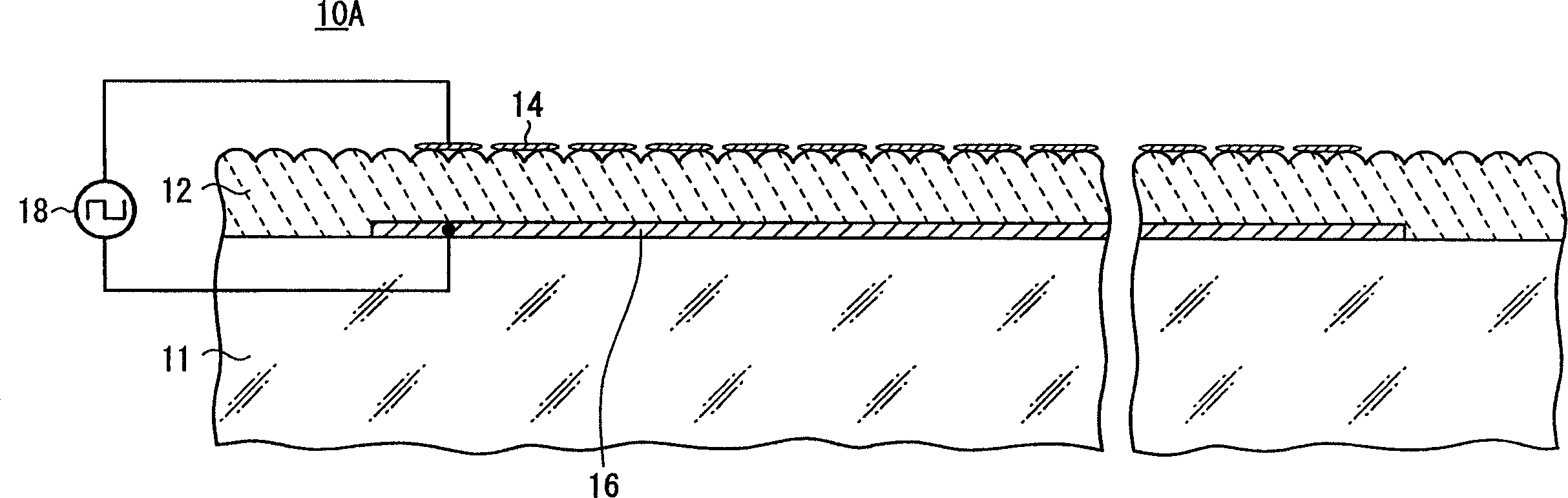
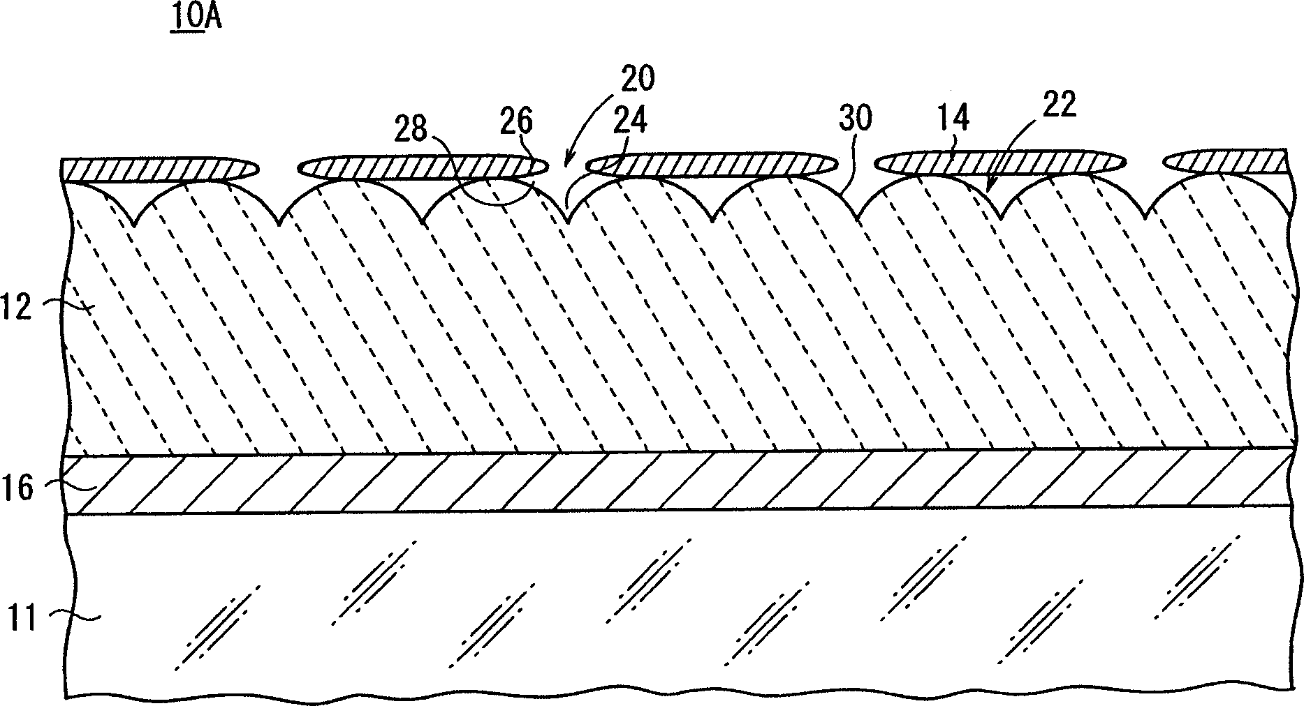
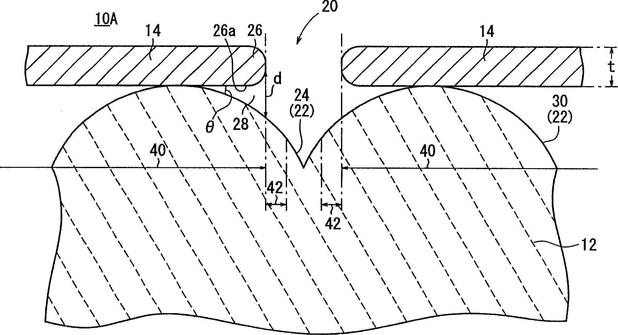
[0076] Refer below Figure 1 to Figure 40 Embodiments of the electron emission device of the present invention will be described.

[0077] First, the electron injection device of this embodiment can be applied to an electron beam irradiation device, a light source, use in place of LEDs, an electronic component manufacturing device, and an electronic circuit component in addition to the use as a display.

[0078]The electron beam in the electron beam irradiation device is superior in absorbing performance at high energy compared with the ultraviolet rays in the ultraviolet irradiation device which is widely used at present. Examples of use include curing insulating films when superimposing wafers in semiconductor devices, uniformly hardening printing inks during printing and drying, and packaging medical devices in boxes for sterilization.

[0079] Applications of light sources include planar light sources such as backlights for liquid crystal displays, and light sources for p...


PUM


Abstract

Electron emitting element with electrode on the glass substrate, the emitting electrode which composed by dielectric film formed on the low electrode and up electrode formed on the emitting electrode. Applying driven voltage for emitting electronic between up-lower electrode. At least the up electrode with multiple through are on the emitting electrode, the edge of the through and surface of the emitting electrode leaved from the emitting electrode.

Description

technical field [0001] The present invention relates to an electron emitting device formed on a glass substrate, an electron emitting device having a plurality of the electron emitting device, a display using the electron emitting device, and a light source using the electron emitting device. Background technique [0002] Recently, an electron emission device having a cathode electrode and an anode electrode is used in various applications such as a field emission display (FED) or a backlight. When FED is applied, a plurality of electron emitting elements are arranged two-dimensionally, and a plurality of phosphors facing these electron emitting elements are respectively arranged at predetermined intervals. [0003] Conventional examples of such electron-emitting elements include Patent Documents 1 to 5, but since they do not use a dielectric in the emitter portion, molding or micro-fabrication is required between opposing electrodes, and it is necessary to apply High volta...

Claims


Application Information

Patent Timeline
Patent Type & Authority Applications(China)
IPC IPC(8): H01J1/312H01J29/04H01J31/12H01J63/02
CPCB82Y10/00H01J2329/00H01J63/02H01J1/312H01J29/481
Inventor 武内幸久七泷努大和田岩
Owner NGK INSULATORS LTD
Why Eureka
Try Eureka