
Image process unit

An image processing and image sensor technology, applied in electrical components, image communication, television, etc., can solve problems such as large incident angle of light, limited effect, sensitivity to too large incident angle of light, etc., to increase sensitivity, overcome The effect of edge falloff

Active Publication Date: 2007-02-21
UNITED MICROELECTRONICS CORP
View PDF0 Cites 8 Cited by
  • Summary
  • Abstract
  • Description
  • Claims
  • Application Information

AI Technical Summary

Problems solved by technology

[0004] It is worth noting that in existing CMOS image sensors, photodiodes of the same size are arranged in an array-type pixel unit or a linear-type pixel unit. As far as the photodiode is concerned, it has a large light incident angle, and because of this, the light incident angle is too large and the sensitivity is reduced
The effect of this edge attenuation (attenuation) directly affects the quality of the image, resulting in a situation where the center is brighter and the edge is darker.
Although in terms of optical compensation technology, the optical signal in the edge area can be enhanced by the focusing of software or microlens, or the effective area of ​​the better photosensitive area can be calculated by the size of the image, but the effect is still limited.

Method used

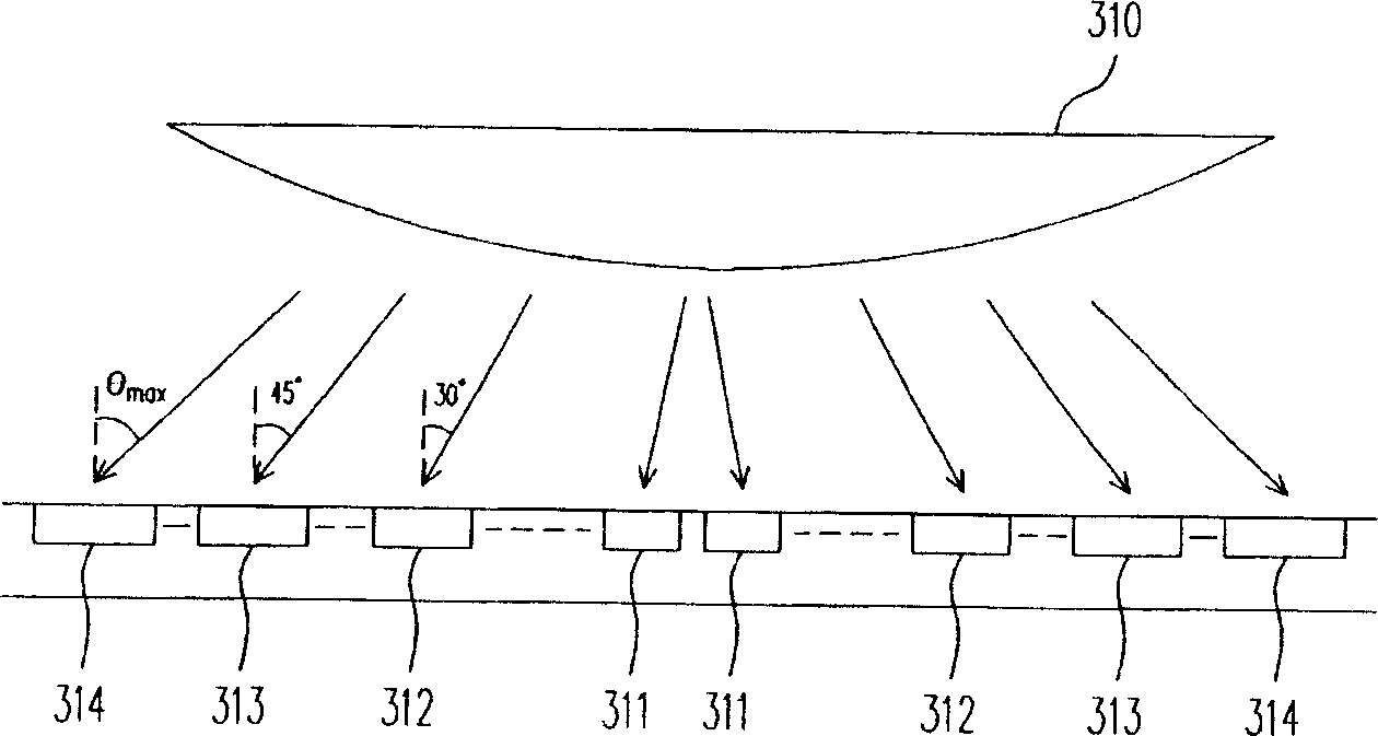

Image

  • Image process unit
  • Image process unit

Examples


Embodiment Construction

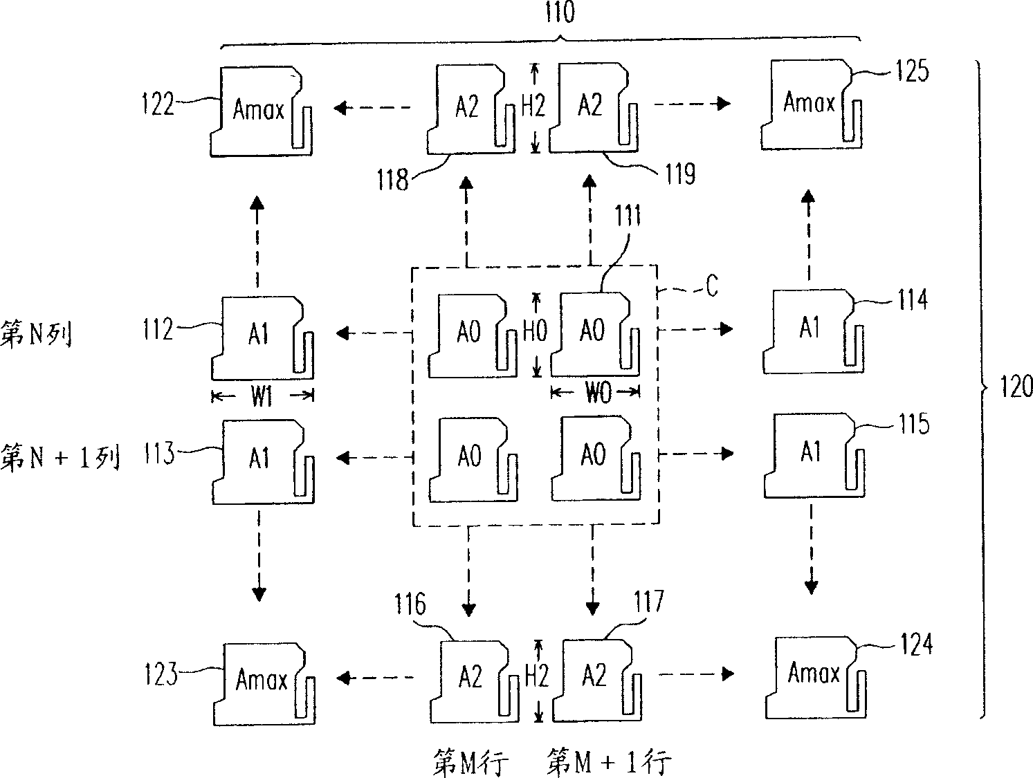
[0027] figure 1 A schematic diagram of an image processing unit according to the first embodiment of the present invention is shown. Regarding the driving method and imaging principle of the image processing unit 100, please refer to the prior art prior to the application for a more detailed description. The following content is only a detailed description of the arrangement and size changes of the image processing unit 100. .

[0028] Please refer to figure 1 , the image processing unit 100 mainly includes a plurality of photodiodes 110 , 120 arranged horizontally and vertically. In terms of arrangement, the photodiodes 110 and 120 can form an array-type pixel unit according to the layout design of semiconductor elements, so as to capture the light signals incident on the photodiodes 110 and 120 and convert them into readable electronic signals. The difference between the present invention and the prior art is that the photodiodes 110 and 120 have photosensitive areas of d...


PUM


Abstract

The invention comprises multi photodiodes lined up in the image sensor; the photodiodes have different sizes of sensing areas due to their different locations and the sizes of their sensing area are gradually increased from central area of the sensor to its edge in order to compensate the low sensibility caused by larger light angle.

Description

technical field [0001] The invention relates to an image sensor, in particular to an image processing unit of a complementary metal oxide semiconductor image sensor (CMOS image sensor). Background technique [0002] A CMOS image sensor is a photoelectric conversion device that can convert an image pattern into a photoelectric signal that can be recognized, processed and stored by a computer through a scanning action. Since the CMOS image sensor uses an integrated photoelectric module to sense the light and shade of the image, compared with the complex optical imaging principle of the charge-coupled device (CCD), it is simpler, easier to assemble, lower cost, and conforms to the product requirements. To meet the requirements of light, thin, short and small times, its applied products include low-end scanners, digital cameras / video cameras and so on. [0003] In image processing, the CMOS image sensor captures images by pixel units composed of photodiodes arranged in an array...

Claims


Application Information

Patent Timeline
Patent Type & Authority Applications(China)
IPC IPC(8): H04N5/335H04N25/00
Inventor 龙赞伦郑志鸿
Owner UNITED MICROELECTRONICS CORP
Learn More