

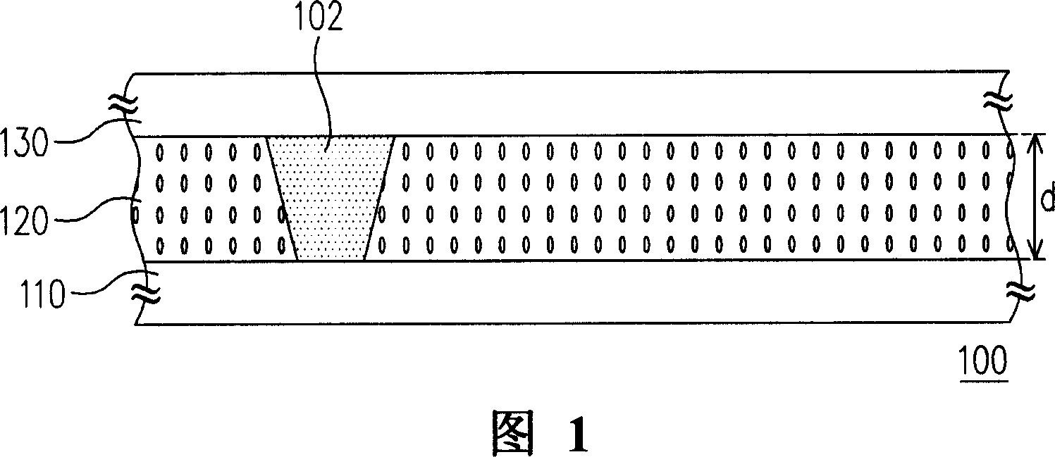
Liquid crystal display board
A liquid crystal display panel, liquid crystal layer technology, applied in nonlinear optics, instruments, optics, etc., can solve the problems of reducing liquid crystal drop injection, bubbles, and the rigidity of the gap support is too strong, so as to improve the process qualification rate and avoid damage effect
- Summary
- Abstract
- Description
- Claims
- Application Information
AI Technical Summary
Problems solved by technology
Method used
Image

Examples
Embodiment Construction
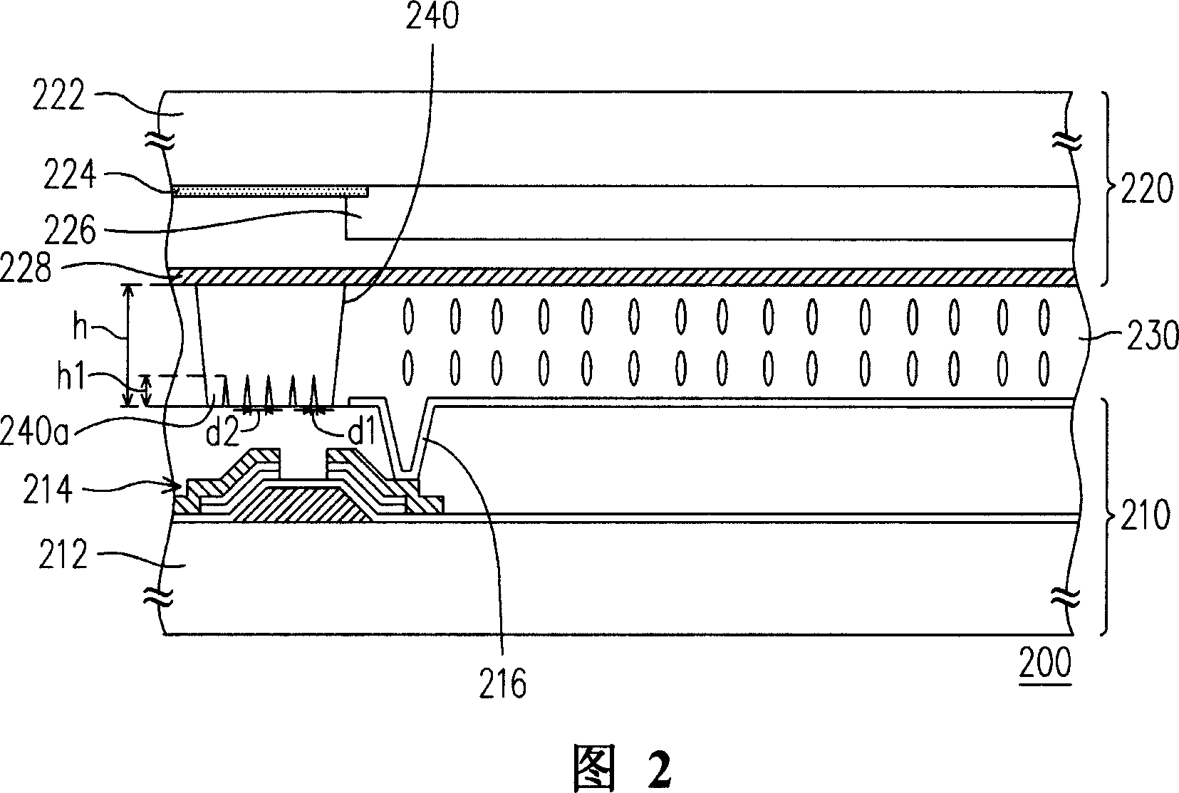
[0049] FIG. 2 is a schematic cross-sectional view of a liquid crystal display panel in a preferred embodiment of the present invention. Referring to FIG. 2 , the liquid crystal display panel 200 is mainly composed of a first substrate 210 , a second substrate 220 , a liquid crystal layer 230 and a spacer 240 . Wherein, the second substrate 220 is disposed above the first substrate 210 . In this embodiment, the first substrate 210 is, for example, an active device array substrate composed of a transparent substrate 212 and a plurality of active devices 214 and pixel electrodes 216 disposed thereon. Moreover, since thin film transistors (thin film transistors, TFTs) have good response speeds, in this embodiment, for example, thin film transistors are used as the active elements 214 for driving the liquid crystal display panel 200 . In other words, the first substrate 210 of this embodiment is preferably a thin film transistor array substrate.
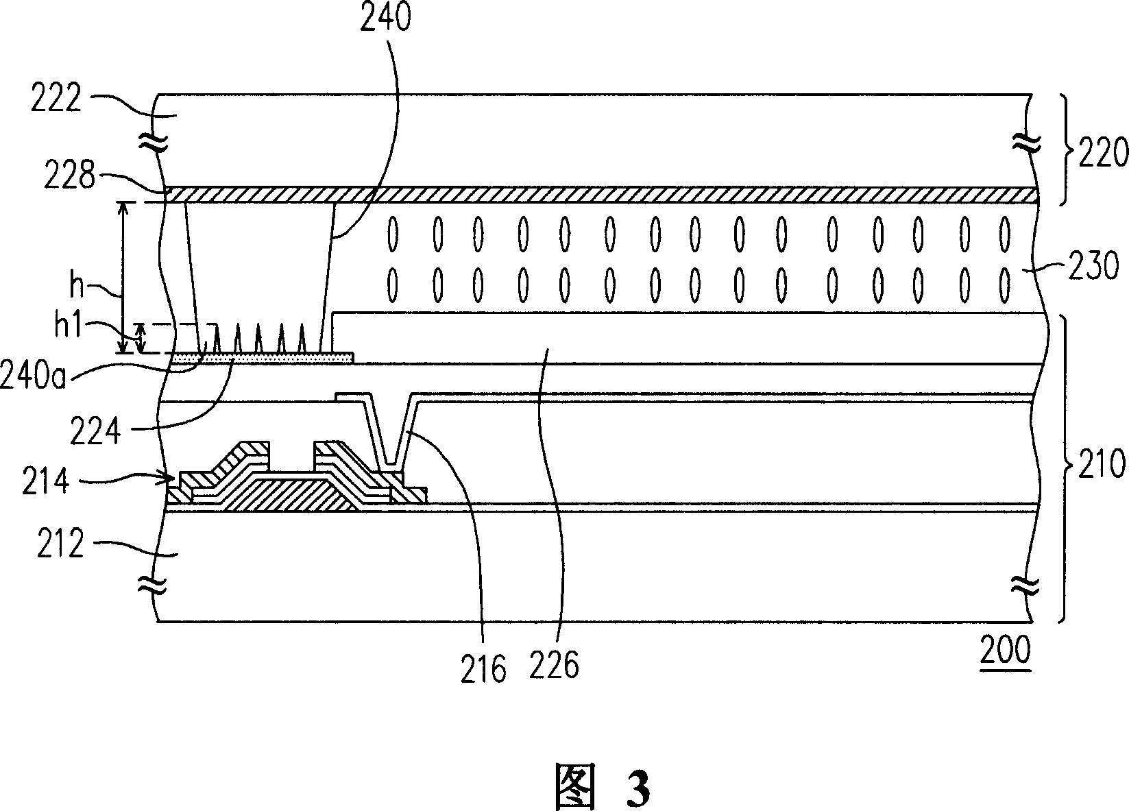
[0050] In addition, the second s...
PUM
 Abstract
Description
Claims
Application Information