Chip washing process and method for forming opening therefor

A wafer cleaning and wafer technology, applied in cleaning methods and utensils, cleaning methods using liquids, chemical instruments and methods, etc., can solve the problems of incomplete cleaning, influence of metal interconnection quality, and reduced yield, etc. Easy to clean and stable wafer cleaning results

Active Publication Date: 2007-03-28
UNITED MICROELECTRONICS CORP
View PDF0 Cites 3 Cited by
  • Summary
  • Abstract
  • Description
  • Claims
  • Application Information

AI Technical Summary

Problems solved by technology

However, for the damascene opening process using a metal hard mask layer, the polymer on the sidewall of the damascene opening on the substrate (wafer) is often not completely cleaned, which greatly affects the quality of the metal interconnection. , so that the yield of the product is greatly reduced

Method used


Image

  • Chip washing process and method for forming opening therefor
  • Chip washing process and method for forming opening therefor
  • Chip washing process and method for forming opening therefor

Examples


Embodiment Construction

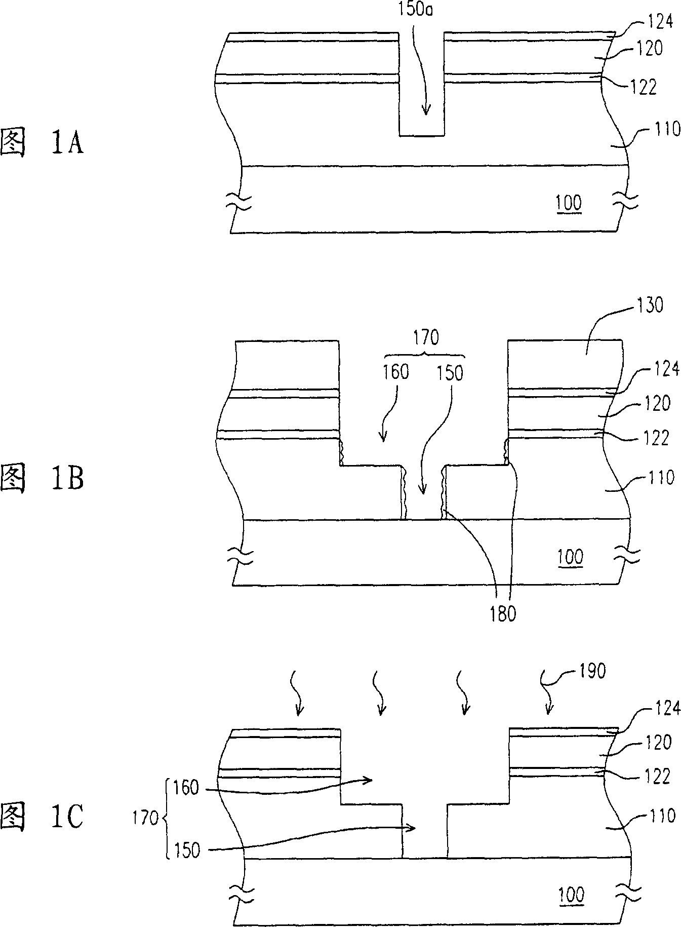
[0044] The preferred embodiment takes the polymer removal step after the etching step of the dual damascene opening as an example, which is not intended to limit the scope of the present invention.

[0045] 1A to 1C are schematic cross-sectional views of a dual damascene opening process. First, please refer to FIG. 1A , a substrate 100 is provided, and the substrate 100 has a plurality of elements (not shown). A dielectric layer 110 is formed on the substrate 100. The material of the dielectric layer 110 is, for example, silicon oxide or silicon-based (silicon-based) low dielectric constant material, such as hydrogen-containing silicate (hydrogen silsesquioxane, HSQ), Methyl silicates (methylsesquioxane, MSQ) and so on. Next, a hard mask layer 120 is formed on the dielectric layer 110, and its material is, for example, silicon nitride or metal. When the hard mask layer 120 is a metal hard mask layer, and its material is titanium nitride (TiN) and other metals, intermediate l...


PUM


Abstract

The technique for cleaning out wafers is suitable to be carried out after an etching procedure is executed for a wafer. The wafer possesses center of circle, radius and edge of a wafer. The method includes operations: a nozzle transfers cleaning solution above the wafer; the nozzle moves along a moving path by using wafer center of circle as center; back and forth movement is carried out above neighborhood of center of wafer.

Description

technical field [0001] The present invention relates to semiconductor processing, and more particularly to a method of removing residual polymer from a wafer. Background technique [0002] In the semiconductor process, the patterning process of a material layer generally includes a photolithography step of forming a patterned photoresist, and an etching step using the patterned photoresist as a mask thereafter. Since the photoresist is organic, after the etching step, there are usually some etching residues composed of polymers left on the substrate, which will cause many problems. For example, in the process of damascene opening, there are usually etching residue polymers formed on the sidewalls of the opening, affecting subsequent processes. For example, in the semiconductor process, if the polymer is not properly removed, it will affect the subsequent metal filling process, and thus reduce the quality of the metal interconnection. [0003] In order to solve the problem ...

Claims


Application Information

Patent Timeline
Patent Type & Authority Applications(China)
IPC IPC(8): H01L21/00H01L21/3105B08B3/00
Inventor 陈博仁
Owner UNITED MICROELECTRONICS CORP
Why Eureka
Try Eureka