Memory
A memory and memory cell technology, applied in the field of memory, can solve problems such as increased interference and disappearance of data
- Summary
- Abstract
- Description
- Claims
- Application Information
AI Technical Summary
Problems solved by technology
Method used
Image

Examples
no. 1 approach
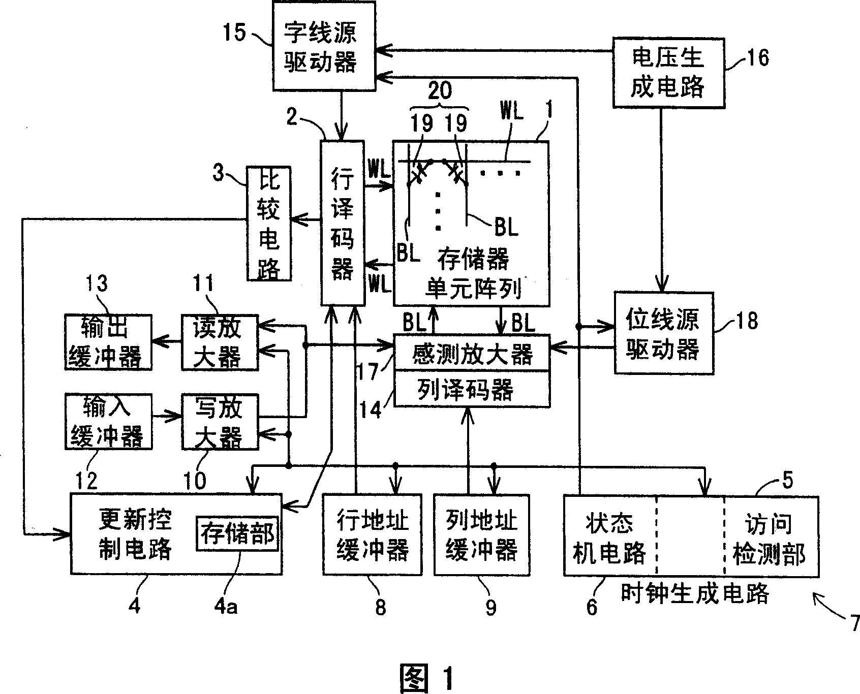
[0044] First, the configuration of the ferroelectric memory according to the first embodiment will be described with reference to FIGS. 1 to 7 .
[0045] As shown in FIG. 1, the ferroelectric memory of the first embodiment includes: a memory cell array 1, a row decoder 2, a comparison circuit 3, an update control circuit 4 with a storage unit 4a, an access detection unit 5 and a state machine circuit. 6 clock generating circuit 7, row address buffer 8, column address buffer 9, write amplifier 10, sense amplifier 11, input buffer 12, output buffer 13, column decoder 14, word line source driver 15, voltage A generation circuit 16 , a sense amplifier (sense amplifier) 17 , and a bit line source driver 18 . In addition, the update control circuit 4 is an example of the "update unit" of the present invention.
[0046] In the memory cell array 1, a plurality of word lines WL and a plurality of bit lines BL are arranged to intersect, and a ferroelectric capacitor 19 is arranged at...
no. 2 approach
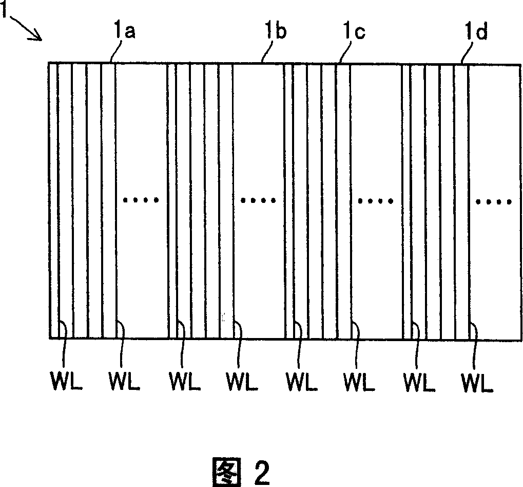
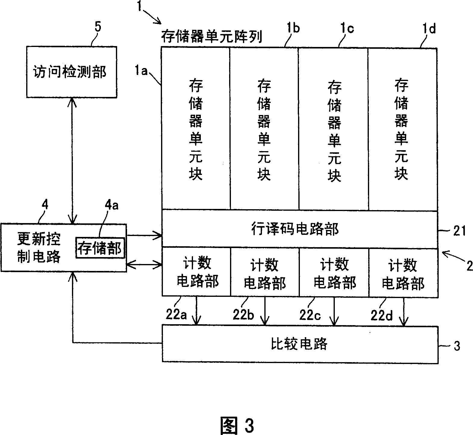
[0095] Referring to FIGS. 10 to 12 , this second embodiment differs from the first embodiment in that it detects the order in which the number of accesses to each of the four memory cell blocks 1 a to 1 d is greater.
[0096] In this second embodiment, as shown in FIG. 10, in the structure of the first embodiment shown in FIG. Each of 1d is in the order of the most number of visits. In addition, the structure other than the comparison circuit 50 of 2nd Embodiment is the same as that of 1st Embodiment mentioned above.
[0097] As shown in FIG. 11, the comparator circuit 50 of the second embodiment is configured to output an output signal MXA as sequence data when the count signals CNTA to CNTD output from the respective counting circuit sections 22a to 22d (see FIG. 10) are input. ~MXD. The output signals MXA to MXD are 2-bit signals, and the output signals MXA to MXD respectively correspond to the memory cell blocks 1a to 1d (see FIG. 10 ). For example, when the number of t...
no. 3 approach
[0131] Referring to FIG. 14 , in this third embodiment, different from the first and second embodiments described above, an example of detecting the number of accesses to all memory cells in the memory cell array 1 will be described.
[0132] In this third embodiment, as shown in FIG. 14, in the configuration of the first embodiment shown in FIG. Counter 61 of times. In addition, the counter 61 is an example of the "second count detection part" of this invention. The counter 61 is configured such that the number of counts is increased by +1 each time an access operation to all the memory cells is detected by the access detection unit 5 .
[0133] Furthermore, in the third embodiment, when the counter 61 detects that the number of accesses to all memory cells in the memory cell array 1 has reached a predetermined number, the update control circuit 4 controls the update operation based on the comparison data output from the comparison circuit 3 .
[0134] In addition, other co...
PUM
 Abstract
Description
Claims
Application Information
 - R&D
- Intellectual Property
- Life Sciences
- Materials
- Tech Scout
- Unparalleled Data Quality
- Higher Quality Content
- 60% Fewer Hallucinations
Browse by: Latest US Patents, China's latest patents, Technical Efficacy Thesaurus, Application Domain, Technology Topic, Popular Technical Reports.
© 2025 PatSnap. All rights reserved.Legal|Privacy policy|Modern Slavery Act Transparency Statement|Sitemap|About US| Contact US: help@patsnap.com