Method and apparatus for operating series nonvolatile memory unit
A non-volatile storage, non-volatile technology, applied in the field of electrically erasable programmable non-volatile memory
- Summary
- Abstract
- Description
- Claims
- Application Information
AI Technical Summary
Problems solved by technology
Method used
Image

Examples
Embodiment Construction
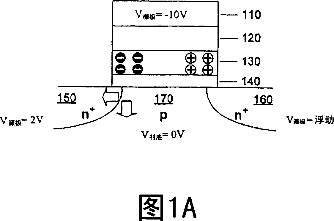
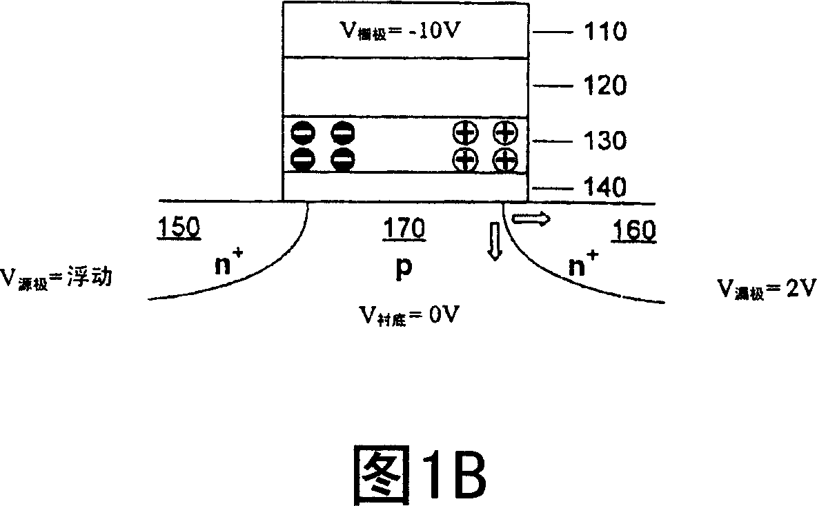
[0067] FIG. 1A is a schematic diagram of a charge trapping memory cell, showing a read operation performed on a portion of the charge trapping structure corresponding to a source terminal. P-type doped substrate region 170 includes n+ doped source and drain regions 150 and 160 . The remaining memory cells include a bottom dielectric structure 140 on the substrate, a charge trapping structure 130 on the bottom dielectric structure 140 (bottom oxide layer), a top dielectric structure 120 (top oxide layer) on the charge trapping structure 130 ), and the gate 110 on the oxide structure (should be a top dielectric structure) 120 . A typical top dielectric structure consists of about 5 to 10 nanometers thick silicon dioxide and silicon oxynitride, or other similar high dielectric constant materials such as aluminum oxide (Al 2 o 3 ). Typical bottom dielectric structures include silicon dioxide and silicon oxynitride, or other similar high dielectric constant materials, about 3 to...
PUM
 Abstract
Description
Claims
Application Information
 - R&D Engineer
- R&D Manager
- IP Professional
- Industry Leading Data Capabilities
- Powerful AI technology
- Patent DNA Extraction
Browse by: Latest US Patents, China's latest patents, Technical Efficacy Thesaurus, Application Domain, Technology Topic.
© 2024 PatSnap. All rights reserved.Legal|Privacy policy|Modern Slavery Act Transparency Statement|Sitemap