Erasing method of single-gate non-volatile memory

A non-volatile, gate technology, used in electrical components, electrical solid devices, circuits, etc., can solve the problems of complex preparation, serious over-erasing of single-gate EEPROM components, and increased labor hours.

Inactive Publication Date: 2007-04-25
YIELD MICROELECTRONICS CORP
View PDF0 Cites 0 Cited by
  • Summary
  • Abstract
  • Description
  • Claims
  • Application Information

AI Technical Summary

Problems solved by technology

Therefore, in the structure of the known non-volatile memory, in addition to the gate layer of the transistor, an additional conductive layer needs to be added to store charges, and the formation of a double-layer structure is more expensive than the general CMOS in terms of preparation. The additional steps of film deposition, etching, exposure and development, etc. increase the cost, complicate the preparation, decrease the component yield, and increase the working hours, especially when it is used in embedded (Embedded) EEPROM products.
[0004] In the known erasing method for EEPROM components, the stored charge is moved from the floating gate to the transistor under the tunneling effect of the Fowler-Nordheim (Fowler-Nordheim) tunneling (referred to as F-N tunneling) technology. Removed, the voltage often needs to be greater than 10V, and because the structure of the single-gate EEMPROM memory is transistor base-floating gate-capacitor base, the stored charge can be released to any direction according to the direction of the electric field; resulting in a single-gate Over-erasing of extreme EEPROM components becomes more serious

Method used


Image

  • Erasing method of single-gate non-volatile memory
  • Erasing method of single-gate non-volatile memory
  • Erasing method of single-gate non-volatile memory

Examples


Embodiment Construction

[0015] In the following, specific embodiments are described in detail with reference to the accompanying drawings, so that it is easier to understand the purpose, technical content, features and effects of the present invention.

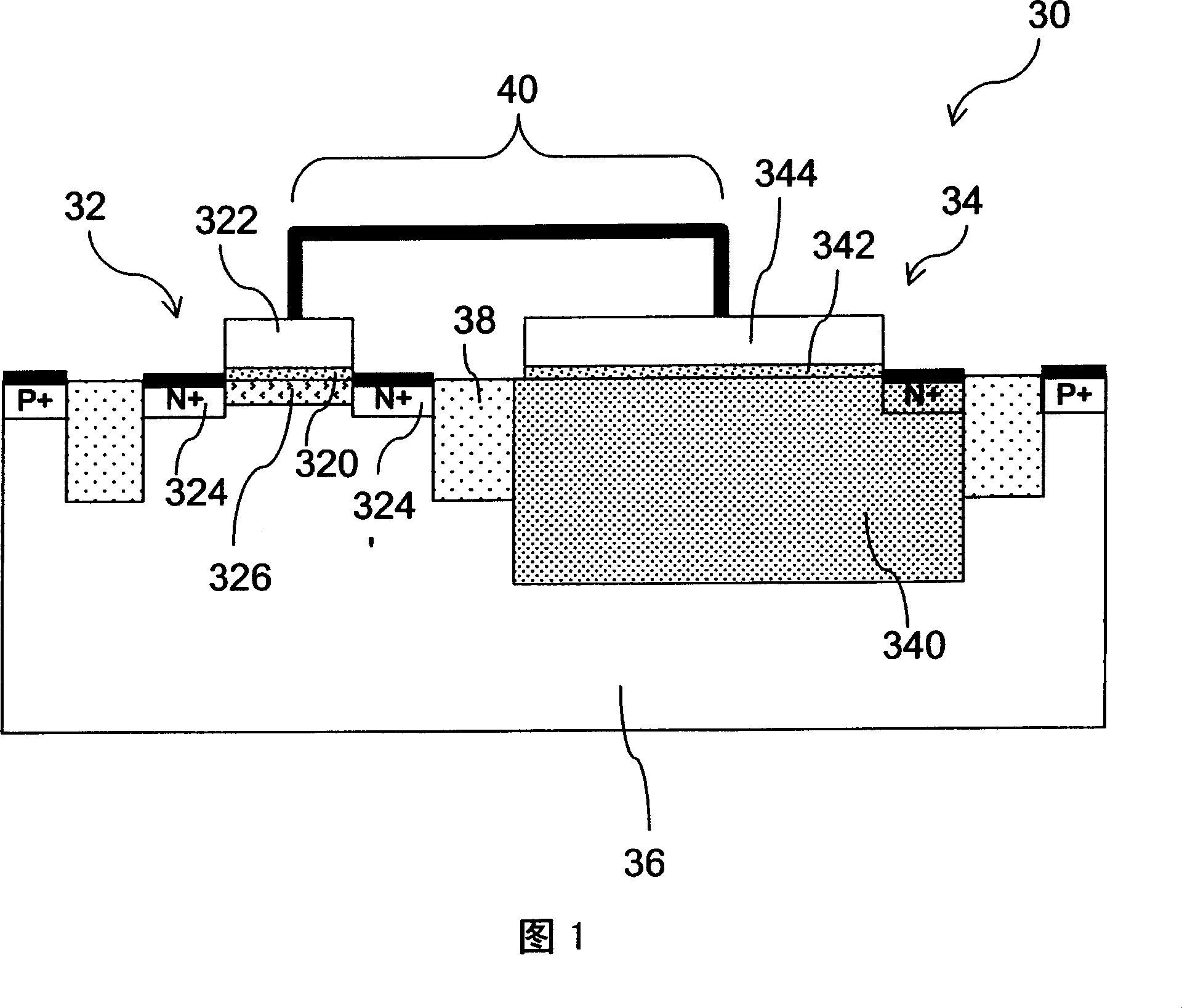
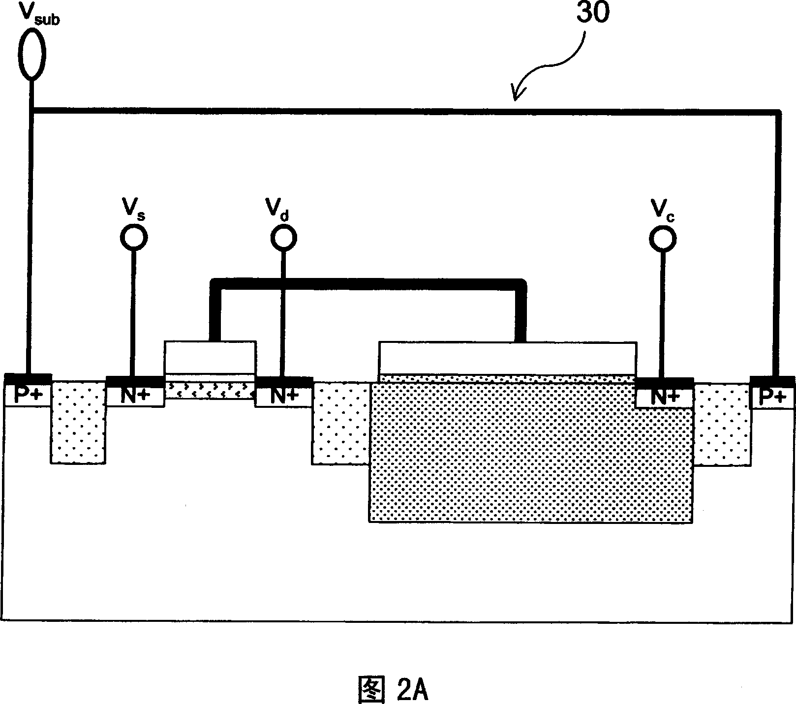
[0016] 1 is a cross-sectional view of the single-gate non-volatile memory structure provided by the first embodiment of the present invention. The single-gate non-volatile memory structure 30 includes an NMOS transistor (NMOSFET) 32 and an N-well (N-well) capacitor 34 in the P-type silicon substrate 36; the NMOS transistor 32 includes a first dielectric layer 320 located on the surface of the P-type silicon substrate 36, a first conductive gate 322 stacked above the first dielectric layer 320, and two N + The ion-doped region is located in the P-type silicon substrate 36, serving as its source 324 and drain 324' respectively, and a channel 326 is formed between the source 324 and the drain 324'; the N-well capacitor 34 includes the second ion-doped re...


PUM


Abstract

The invention relates to a method for erasing single-gate non-volatile memory. Wherein, it has single flow gate polar structure; when it erases, it functions voltage on door polar to generate reverse layer. The invention can reduce erasing voltage and improve erasing speed, and it can avoid over erase.

Description

technical field [0001] The present invention relates to a non-volatile memory (Non-Volatile Memory), in particular to a method for erasing a single-gate non-volatile memory that can be erased at low voltage (lower than 10V). Background technique [0002] Press, complementary metal oxide semiconductor (Complementary Metal Oxide Semiconductor, CMOS) preparation technology has become a common manufacturing method of application specific integrated circuit (ASIC). Today, with the development of computer information products, Electronically Erasable Programmable Read Only Memory (Electrically Erasable Programmable Read Only Memory, EEPROM) has the function of electrically writing and erasing data due to its non-volatile memory function, and after the power is turned off, the data It will not disappear, so it is widely used in electronic products. [0003] Non-volatile memory is programmable to store charge to change the gate voltage of the memory's transistors, or not store char...

Claims


Application Information

Patent Timeline
Patent Type & Authority Applications(China)
IPC IPC(8): H01L27/105
Inventor 黄文谦张浩诚
Owner YIELD MICROELECTRONICS CORP
Why Eureka
Try Eureka